ABSTRACT
A fully differential opamp suitable for very-low voltage switched-capacitor circuits in standard CMOS technologies is introduced. The proposed two stage opamp needs a simple low voltage CMFB switched-capacitor circuit only for the second stage. Due to the reduced supply voltage, the CMFB circuit is implemented using bootstrapped switches. Minor modifications allow to use chopper stabilization for flicker noise reduction. Two different compensation schemes are discussed and compared using an example for 1V operation of the amplifier.
1. INTRODUCTION
The increasing interest in low-voltage, low-power integrated circuits has lead to modifying the existing circuit techniques in order to be able to work correctly under these new constraints. In switched-capacitor circuits, reducing the supply voltage increases drastically the switch resistance.
One technique to overcome this problem is clock voltage multiplication. This however is not power efficient and not compatible with very advanced low-voltage CMOS processes where gate oxide breakdown becomes an issue.
Some designs use low threshold transistors for the switches. Obviously, a special process is required. Alternatively, the switched-opamp technique (SO) [1] has been proposed to get around this problem. However, the circuit becomes more complicated and loses some of the speed. This results in relatively poor performance of the switched-opamp circuits.
In [2] a bootstrapped switch is introduced that allows rail-to-rail operation of a single n-switch in a standard CMOS process. Together with using different common mode (CM) voltages at the input and the output of the opamp, this leads to possible rail-to-rail operation of very low-voltage switched-capacitor circuits with the least modifications introduced to existing designs and in the same time enhancing the linearity performance due to the constant drive of the bootstrapped switches [2]. This shift of the CM voltage could be achieved either by injecting a fixed amount of charge at the opamp input at each clock cycle [2], or by using different reference voltages at the input and output of the differential switched-capacitor integrator as shown in Fig. 1. Both the input signal and the amplifier output has a CM voltage equal to Vcm-out which is usually chosen near the mid-supply range in order to maximize signal excursions. Bootstrapped switches are thus used to switch signals around Vcm-out. On the other hand, the amplifierinput CM voltage is at Vcm-in which is near V SS such that single n-switches are sufficient.

Since reduced supply voltage forces current consumption to increase [3], the amplifier topology plays a critical role in low-voltage, low-power switched-capacitor design. Additional circuitry for common-mode operation must also be considered in the same time so as not to degrade the overall amplifier performance.
In [4] a 1V two-stage amplifier is designed for the SO technique. It is based on a p-type folded-cascode two stage Miller-compensated structure. An additional common-mode amplifier, also performing the necessary signal inversion, is used for the CMFB. The overall opamp operates at a minimum supply voltage of VGS +VDSsat, but speed and power consumption are both limited by the additional CMFB amplifier.
In [5], the same opamp is used but with the CMFB in the first stage implemented using a cross-coupled transistor stage. CMFB in the second stage is achieved using a simple passive circuit suitable only for SO circuits. The minimum supply voltage needed is however increased by one VDSsat.
This paper introduces further modifications to the above cross-coupled connection so as to reduce the minimum supply voltage. Bootstrapped switches allow a simple switchedcapacitor CMFB circuit to be used. Two compensation schemes are considered and compared with respect to the amplifier performance. As the signal level is reduced for reduced supply voltages, the noise level becomes more critical. Special noise reduction techniques are discussed for the modified architecture.
The paper is organized as follows: Section 2 introduces the modified opamp structure. In section 3, simulation results are shown comparing the two possible compensation schemes. Finally, conclusions are summarized in section 4.
2. PROPOSED OPAMP
For the differential opamp shown in Fig. 1, the low supply voltage prevents the use of stacked transistors so that a twostage amplifier is usually needed to achieve the required dc gain.
An input PMOS differential pair allows the use of V SS as the opamp CM input voltage Vcm-in.
2.1. Common-Mode Feedback
Due to the differential structure, the common mode output voltage of both stages needs to be regulated using CMFB. Biasing of class-A amplifiers is typically accomplished with a CMFB circuit that senses the output CM voltage in order to control the tail current source via a current mirror. However, owing to stability considerations, the gain and bandwidth of the CMFB loop are limited to at most those of the differential mode signal path. Moreover, power consumption is increased due to the added CMFB circuitry.
Fig. 2 shows the proposed amplifier structure. The NMOS cascode current source has been split into two equally-sized, cross-coupled devices (M51, M52 and M61,M62) with their gates connected to the two outputs of the first stage (nodes n3 and n4). This negative feedback connection causes the differential signal at the output of the first stage (nodes n3 and n4) to see a high load impedance given by the reciprocal of


The conductance gm51 seen at the gate of transistors M51 and M61 is thus canceled by the opposite action of the parallel transistors M52 and M62 respectively. Proper matching of these transistors, together with other terms in equation (1) prevent the output resistance from going negative. The total conductance gdsout1 is thus limited by gds8.
On the other hand, for the common mode signal, the output conductance is also given by equation (1) but with the negative term turned positive. The total conductance gdsout1 in this case is limited by gm51 + gm52. This impedance is a low one and thus the first stage does not require an additional CMFB circuit. In fact the cross-coupled devices act like a built-in CMFB circuit that senses the output of the first stage and regulates its common mode voltage. It also allows a minimum supply voltage of VGS + VDSsat.
The second stage is composed of the NMOS common source amplifier M11(M13) with active load M10(M12). A simple passive switched-capacitor CMFB circuit (shown in Fig. 1) can be used in this case. The dc voltage across C1 is determined by capacitor C2 which is switched between being in parallel with C1 and Vcm-out-Vb, where Vb is the desired biasing voltage for the current source ptransistors M10 and M12. Since the potential Vb is close to V SS, n-transistors can be used to switch it. However, bootstrapped switches must be used in the CMFB circuit for those switches that have to switch the Vcm-out potential.
These bootstrapped switches can be shared with the sampling network connecting the integrator output to subsequent stages as shown in Fig. 1.
2.2. Opamp Compensation
Two possible compensation schemes are possible for this two-stage opamp structure: The first one is the standard Miller compensation scheme which consists of connecting the compensation capacitor CC in series with a compensation resistance RC between the output nodes and the output of the first stage (nodes n3 and n4). Analysis of the amplifier shows that the transfer function has five poles and two zeros that can be placed in the half-left plane. A sort of pole-zero cancellation is also possible by properly choosing the value of RC. This further enhances the phase margin.
The second compensation scheme is shown in Fig. 2. This is done by connecting the compensation capacitor CC to the source of the cascode devices (nodes n1 and n2) [6]. These low impedance points decouple the gate of the output stage amplifier (transistors M11 and M13) from the compensation capacitor. This technique offers a much improved highfrequency power-supply rejection ratio (PSRR) and moves the right-half plane zero resulting from Miller compensation into high frequencies. It can be shown [6] that this type of compensation results in two complex poles besides the dominant one. It is thus quite possible to obtain a design with adequate phase margin, which suffers from insufficient gain margin due to gain peaking beyond the unitygain bandwidth, caused by a high pole quality factor Qp. This pole quality factor Qp is given by [6]

It can be kept low by making the transconductances of the cascode transistor M3(M4) large compared to the output driver M11(M13). In addition a moderate value of CC is required.
Both schemes ensure stability. Low-Qp considerations for the second one usually impose more constraints on the design of the amplifier. High cascode transconductance implies either lower VGS-Vth or higher current. Lower VG-Vth leads to higher parasitic capacitance which will reduce the amplifier bandwidth. This implies an optimum VGS-Vth value. Higher cascode current implies larger power consumption and higher input referred thermal noise. In addition, the value of the compensation capacitance CC in the second case is limited by the required Qp. Since the aliased input referred in-band white noise in switched-capacitor circuits is inversely proportional to the value of the compensation capacitor of the amplifier, this restricts the white noise performance optimization.
2.3. Noise Reduction
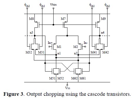
For low-noise input front-ends, the input amplifier noise optimization is an important step in the overall system design. Thermal noise can be reduced using higher input current in the input differential pair. While flicker noise can be reduced using larger areas for the transistors contributing to the flicker noise (namely M1, M2, M5, M6, M8 and M9). This causes higher parasitic capacitance on the internal nodes and thus increases the amplifier power consumpch2 tion. To overcome this, techniques such as chopper stabilization [7] can be used. For the proposed amplifier, the input is chopped using four input n-switches as shown in Fig. 1. On the other hand, the output of the first stage is chopped as shown in Fig. 3 using only two additional cascade transistors M32 and M42 in parallel with the existing ones but with their sources connected to nodes n2 and n1 respectively. The gates of both cascodes are then driven by two overlapping chopper clocks (Øch1 and Øch2) at half the sampling frequency. The two chopper clocks must overlap to avoid the simultaneous cutoff of both cascodes in parallel in the same time which would increase the settling time of the opamp. Using the supply as the gate bias of the cascade transistors eliminates the need of an additional biasing voltage. This arrangement reduces the 1=f noise for all transistors but M8 and M9 where a larger transistor length must be used.
Both schemes ensure stability. Low-Qp considerations for the second one usually impose more constraints on the design of the amplifier. High cascode transconductance implies either lower VGS-Vth or higher current. Lower VG-Vth leads to higher parasitic capacitance which will reduce the amplifier bandwidth. This implies an optimum VGS-Vth value. Higher cascode current implies larger power consumption and higher input referred thermal noise. In addition, the value of the compensation capacitance CC in the second case is limited by the required Qp. Since the aliased input referred in-band white noise in switched-capacitor circuits is inversely proportional to the value of the compensation capacitor of the amplifier, this restricts the white noise performance optimization.
2.3. Noise Reduction
For low-noise input front-ends, the input amplifier noise optimization is an important step in the overall system design. Thermal noise can be reduced using higher input current in the input differential pair. While flicker noise can be reduced using larger areas for the transistors contributing to the flicker noise (namely M1, M2, M5, M6, M8 and M9). This causes higher parasitic capacitance on the internal nodes and thus increases the amplifier power consumpch2 tion. To overcome this, techniques such as chopper stabilization [7] can be used. For the proposed amplifier, the input is chopped using four input n-switches as shown in Fig. 1. On the other hand, the output of the first stage is chopped as shown in Fig. 3 using only two additional cascade transistors M32 and M42 in parallel with the existing ones but with their sources connected to nodes n2 and n1 respectively. The gates of both cascodes are then driven by two overlapping chopper clocks (Øch1 and Øch2) at half the sampling frequency. The two chopper clocks must overlap to avoid the simultaneous cutoff of both cascodes in parallel in the same time which would increase the settling time of the opamp. Using the supply as the gate bias of the cascade transistors eliminates the need of an additional biasing voltage. This arrangement reduces the 1=f noise for all transistors but M8 and M9 where a larger transistor length must be used.
It should be noted that the input chopper switches, shown in Fig. 1, create an additional pole together with the input capacitance of the opamp. This pole must be considered during the amplifier design.
3. RESULTS
As an example of the proposed architecture, table 1 shows the simulated results of two sized netlists. The first using the cascode compensation scheme, and the second (shown between brackets for different values) using the Miller scheme with a nulling resistor to compensate for the right half-plane zero. Both circuits are sized for the same supply voltage, unity-gain frequency, phase margin, slew rate, and output voltage range in order to be able to compare them. A 0.35_ technology is used with a p- and n-transistor thresholds of 0.63 V and 0.6 V respectively. It is to be noted that for the CMFB network shown in Fig. 1, the capacitor C1 loads the amplifier output. At the same time, it is connected to the Vcmfb input of the amplifier which has an input capacitance equal to double the gate ca pacitance of M10. A capacitor divider thus exists and some gain of the CMFB network is lost. To overcome this problem, C1 is chosen to be five times the size of the input capacitance at Vcmfb. During sizing this capacitance is limited to 20% of the load capacitance.

For the cascode compensation scheme, a lower compensation capacitance value could be used, this reduces the overall power consumption. However, due to low-Qp considerations it is more difficult to obtain a satisfactory gain. The high-frequency PSRR is also better for cascode compensation. Careful layout can further enhance the PSRR performance for both cases as supply noise is considered as a CM signal and is cancelled at the differential output of the amplifier.
Additional transistors for chopper stabilization are taken into account during sizing. Flicker noise can thus be neglected. Fig. 4 shows the simulated open-loop gain for both cases, gain peaking can be easily identified for the cascade compensation case. Special care has been taken during sizing such that the complex pole quality factor Qp does not exceed unity.
Additional transistors for chopper stabilization are taken into account during sizing. Flicker noise can thus be neglected. Fig. 4 shows the simulated open-loop gain for both cases, gain peaking can be easily identified for the cascade compensation case. Special care has been taken during sizing such that the complex pole quality factor Qp does not exceed unity.

4. CONCLUSIONS
The proposed fully differential opamp allows very low supply voltage operation and minimizes the additional CMFB circuitry thus saving the overall power. Conventional Miller and cascode compensation schemes are compared using a design example. Minor modifications allow the chopper-stabilization technique to be used for noise reduction. Combined with the switch bootstrapping technique, the proposed architecture permits robust very-low voltage switched-capacitor circuits to be constructed in standard CMOS technologies using common design techniques.
Hernández Caballero Indiana
Asignatura: CAF
Fuente: http://citeseerx.ist.psu.edu
No hay comentarios:
Publicar un comentario