Abstract—This report presents a fully differential operational amplifier (opamp) for a pipeline analog-to-digital (ADC) with high gain (110 dB), ample phase margin (67.8°), low input capacitance ( 1.5 pf) and fast settling time (29.03ns) designed in a 2.5 V, 0.250 um CMOS process. The opamp consumes 59.2mW of power and 800um x 400um of area. The opamp’s performance was verified over 0-100 C and three process corners.
Index Terms—common mode feedback, gain enhancement, opamp, pipeline ADC
I. INTRODUCTION
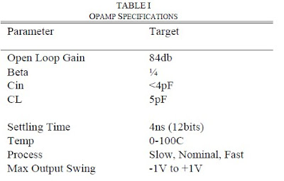
HIS report presents a fully differential opamp designed for a pipeline ADC stage. Table 1 highlights the specifications for the design. The implementation of this design must have high gain and a fast settling time. The quickness of opamp settling determines the speed of the pipeline ADC, thus fast settling is desirable. The higher the gain of an omamp the more ideal it is, and in feedback gain approaches 1/β with less error. [1] presents a design with high gain and high unity gain bandwidth though their implementation was in a significantly different process than ours. The authors present a differential folded cascode amplifier with gain enhancement, as well as presenting relevant background on gain enhancement. The authors were able to achieve a gain in excess of 90 dB, which exceed the specification for our project. We therefore chose the enhanced folded cascode architecture as the basis of our design
The folded cascode provides the needed headroom for an output swing in excesss of 1Vpk. With enhancement a high gain is possible, as [1] showed.
III. CIRCUIT DESCRIPTION
A. Architecture
Figure 1 highlights the architecture of the opamp that was designed. A fully differential in and out amplifier was
realized. A folded cascode differential amplifier was chosen in order to support the specified output swing of 2 volts peak to peak.. The folded cascode design was also selected for its high output impedance. Bias current is mirrored with PMOS devices across the top of the schematic. Gain enhancement boost amps were designed and implemented to increase the output impedance of the folded cascode and meet specified gain. PMOS inputs were selected to minimize the capacitance at the drain node of the input devices, as NMOS are more area efficient, to improve phase margin. Bias voltages are generated in the block I33 using ratios of NMOS and PMOS sizing. Finally, common mode feedback was implemented in order to improve output swing.
B. Gain Enhancement
Figure 2 highlights the architecture of the gain enhancement that was implemented. A differential in single ended out opamp with gain A works to resist changes in the gate source voltage of M2 increasing the effective output resistance of the cascode of the by A. The gain enhancement also adds robustness to temperature and process variation. The gain boost opamp positive terminal takes a reference voltage that can be selected to ensure the drain source voltage of M1 remains large enough to ensure M1 stays in the saturation region which gives the highest output impedance.
The gain boost amplifiers were implemented with single ended output folded cascode opamps as shown in [4].
D. Common Mode Feedback
Common mode feedback is necessary to regulate the common mode of the differential outputs of the opamp to ensure a large output swing. In figure 1 the common mode feedback circuit block is within the center of the two halves of the folded cascode. A simplified schematic of the common mode feedback circuit can be seen in figure 3. The current sources in the figure represent the pmos current mirrors. Vout+ and Vout- are the outputs of the enhanced folded cascode. Vset is a reference voltage that needs to be insensitive to temperature and process variations, to ensure constant common mode output. Vset is generated using two equally sized NMOS as a voltage divider to set VSET ideally to half of VDD. The diode connected NMOS is used to mirror current back into the folded cascode stack.
The circuit operates as follows: as the output common mode rises more of the current from the current sources is sunk through the outside legs of the circuit, and thus through the diode connected NMOS current mirror at the bottom of the circuit. This increase in current through the NMOS causes an increase in current within the folded cascode stack, forcing the output common mode to fall. Thus a form of negative feedback exists that regulates the output common mode.
IV. CIRCUIT ANALYSIS
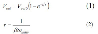
The most challenging target specification was the 12bit settling time of 4ns. According to equation (1) and (2) a unity gain frequency of 1.3GHz is necessary to meet this specification.
Using our output capacitance specification of 5pF in equation (3) the required gm of the input PMOS was calculated to be 6.5mS.
Using the gm of 6.5mS, we solved for the output impedance necessary in a non-boosted folded cascode to obtain a gain of 84dB. Drain current values through the drivers and the cascode devices were found using simplified hand calculation expressions for gm and rO and assuming all devices would operate in saturation. Device were initially sized using the MOSFET current equation and the drain current values that we calculated.
When this design was initially implemented, all devices operated in the correct region but gain, at approximately 40dB, was much lower than required. Common mode output voltage was also around 2V for each half circuit which would not allow the circuit to swing over the output range we desired. To overcome these shortcomings gain boost amplification and common mode feedback was added to the circuit. Design of the boost amps was based off of the sizings already generated for the fully differential circuit, but with current mirroring between half circuits to make the design differential in / single ended out. Design of the common mode feedback was based on of the NMOS folded cascode CMFB used in [2].
Implementation of CMFB and gain boosting gave us a circuit with an output DC voltage of around 1.25V which allowed the output to swing farther than required. It also resulted in a surplus of gain, producing around 120dB. Our unity gain frequency started out at around 250-300MHz in our intial design when driving the 5pF load cap. Increasing gm of the input transistor was used initially to raise this value, but when used alone the sizing of this device became impractical and capacitive loading of internal nodes by this device became pronounced. To push out ωunity we systematically scaled down the lengths and overall W/L ratios of devices connected to the output node and the intermediate cascode node. This allowed us to achieve a nominal ωunity of around 850MHz into the 5pF load with good single pole behavior throughout the amplifiers frequency response. An optimal input driver size was found such that scaling the driver down hurts performance and scaling the driver up yields no significant gains and a large area and power consumption cost.
To achieve stability and an acceptable phase margin the unity gain frequency of our boost amps needed to be slowed from their initial state. This was accomplished by attaching a capacitive load of 4.5pF to the output of each boost amp. This did not negatively affect overall ωunity and gave us a good 60-70 degree worst case stability (β = 1) phase margin for the overall circuit.
Our final design was very robust overs changes in bias voltage so biases were set with simple resistive divider circuits using diode connected PMOS and NMOS devices. The most important bias voltage for op-amp operation was Vset, the input voltage to the common mode feedback. This voltage was set using a divider of two identical diode connected NMOS devices so it does not depend on an N to P ratio to set its value.
V. RESULTS
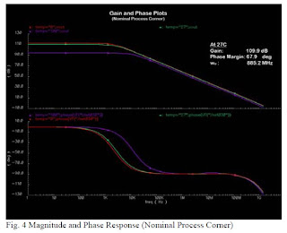
The fully differential opamp was designed in Cadence and simulated over slow, nominal, and fast process corners and at 0°, 27°, and 100° C. Layout of the device was also completed, and all presented results include extracted parasitics. Figure 4 below shows the open loop magnitude and phase plot. A fully differential frequency dependant input was swept to determine gain, unity gain freq, 3 dB bandwidth, and phase margin. Phase margin was measured for unity gain feedback to measure worst case stability. Simulated gain exceeded the target of 84 dB, with a value of 110 dB at 27 C. Unity gain bandwidth was 885 MHz which is less than 1.3 GHz target for a theoretical 12 bit settling time of 4 ns, for nominal process and 27 C.
Transient analysis was also completed to measure output swing, and settling time. Transient analysis was completed with inverting feedback with a feedback factor of ¼, as shown in figure 5. Ideal feedback was implemented by using a voltage controlled voltage source with unity gain to decouple the output of the opamp from the feedback network. A resistive divider network of 1kΩ and 3kΩ, giving a beta of ¼ and an ideal gain of 3. Figure 6 shows a transient response focusing on the rising edge of the output for a differential switch in the input. There is not ringing in the output as expected for a unity gain feedback phase margin of 67°. Phase margin > 60° was achieved for all process corners and temperatures. This the opamp has sufficient phase margin to ensure stability. The feedback factor of ¼ also adds to this stability. (Add schematic) Settling time was measured over all process corners and 0,27, and 100 °C. The 12 bit settling time for the average case (27 °C, nominal process) was measured with the settling time calculator in Cadence to be 29.03 ns. The best 12 bit settling time measured was 17.99 ns (0 °C, nominal process). The worst 12 bit settling time measured was 91.65 ns (0 °C, slow process). All measured settling times were greater than the target of 4 ns for this project.
The output swing specification of 1 Vpk was met over all process corners and temperatures. Output swing was verified by checking to ensure that the opamp was not railing out and that an output swing greater than 1 Vpk could be achieved. Figure 7 shows an output swing greater than 1 Vpk (27 °C, nominal process). Stability of the opamp at this operating point is also evident. Table II highlights the 10 bit settling time, unity gain bandwidth, gain, and phase margin over all temperature and process corners considered. Target settling time of 4 ns for 12 bits was specified, but 10 bit settling time was also measured with cursors in Cadence. Data is reported to show variance with process and temperature.
Table III provides a performance summary of the opamp for the average case (27 °C, nominal process).
Figure 8 shows the device layout. It closely follows the schematic and fits in an area of 800umx400um. Routing is restricted to metals 1 through 3 avoids routing over devices. The layout is DRC and LVC clean.
VI. CONCLUSION
A fully differential opamp for a pipeline ADC was realized with an enhanced folded cascode opamp with high gain (110 dB), ample phase margin (67.8°), low input capacitance ( 1.5 pf) and fast settling time (29.03ns) for nominal process corner, 27° C The opamp consumes 59.2mW of power and 800um x 400um of area.
The design met specs for output swing(>1 Vpk), input capacitance (<4pf), and phase margin(>60°) for all process corners and temperatures. Thus design was sufficient output swing and stability all tested operating conditions. The design exceeded the spec for gain (> 84 dB) for all process corners except for the case of slow process and 100°C. Thus gain is very stable over many operating conditions.
The design was unable to meet the target 12 bit settling time of 4 ns over any process corners and temperatures. This is where the design could be improved. This design would have better settling behavior or a smaller load cap. If there was room for greater input apacitance ore transconductance could have been realized increasing the unity gain requency and potentially further reducing the settling time.
Hernández Caballero Indiana
Asignatura: CAF
Fuente:http://www.eecs.umich.edu/~mpflynn/teaching/design_contest/fall_2005/reports/group4_eecs413_F05.pdf


No hay comentarios:
Publicar un comentario