Abstract
A continuous-time common-mode feedback circuit (CMFB) is presented. A two-stage high-gain architecture is used to minimize the offset of the common-mode voltage. A special compensation scheme enables this circuit to be used in high-impedance current-mode systems without a stability problem. Simulation and testing results show the superior performance of this circuit. It is proven to be an ideal common-mode feedback circuit for systems which require an accurate and stable common mode voltage. This circuit has been implemented in a continuous-time switched-current Σ∆ modulator with a 2um CMOS process. With a 50MHz clock, the modulator has achieved a 60dB dynamic range in a 1MHz bandwidth.
1. Introduction
Common-mode feedback circuits (CMFB) stabilize common-mode voltages for fully-differential analog systems by means of adjusting the common-mode output currents. The two differential output voltages are averaged (VCM) and compared with the common-mode reference voltage (VRCM), and the differential voltage is converted to the common-mode output current to adjust the common-mode voltage (VCM). Three different techniques have been used for implementing CMFBs:
* Switched-capacitor
* Differential difference amplifier (DDA)
* Resistor-averaged circuit
Suffering from clock-induced noise, switched capacitor common-mode feedback circuits are suitable only for sampled-data circuits [1][2]. Common-mode feedback circuits implemented by differential-difference amplifiers (DDA) use four identical transistors to average and compare the common-mode voltages [3]–[6]. Due to the limited input range and nonlinearity of the differential pairs, DDA CMFBs can work only for circuits with small voltage swing. The input range and linearity can be improved, however, by reducing the aspect ratios (W/L) of the CMOS transistors or increasing the bias current source. Resistor-averaged common-mode feedback circuits use resistors to average the two differential outputs and send the result to a differential pair to compare with VRCM [7][8]. This technique reduces the common-mode voltage error caused by the nonlinearity of the differential pair. The voltage swing ranges are not limited by the differential pair, and hence, more voltage swing is allowed without a significant offset of common-mode voltage.
The disadvantage of the resistor-averaged CMFB is the requirement of large-valued resistors. Not only do these resistors require more silicon area, but they also load down the output and cause a reduction of the gain. Moreover, they affect output impedances, which are very critical in current-mode systems since they influence the pole and zero locations.
One important performance factor of common-mode feedback circuits is the transconductance gain (ACMFB). ACMFB is equal to the open-loop common-mode output current (IOCM) divided by the voltage difference (VERR) between the common-mode output voltage(VCM) and the common-mode input reference voltage(VRCM).

With a large ACMFB, a smaller common-mode error voltage (VERR) and a faster response can be achieved. For most of the continuous-time CMFB circuits, single-stage structures are used [3][4][5][7]. For single stage DDA CMFBs[3][4][5], if the nonlinear effect of the differential can be ignored, the CMFB circuits can be simplified as shown in Figure 1. For single-stage resistor averaged CMFBs[7], the CMFB circuits can be simplified as shown in Figure 2. The differential output current is then mirrored to the output as the common-mode output current.


From Figure 1 and Figure 2, we find the transconductance of a single-stage CMFB is roughly equal to the transconductance gain of a differential pair. The typical transconductance gain for a differential pair is in the range of 10_A/V to 100_A/V. A 1_A common-mode offset current applied on the output causes a 10mV to 100mV common-mode error voltage (VERR). Some systems may not tolerate this amount of common-mode voltage offset. One solution to improve the transconductance gain is to use a two-stage architecture [6][8]. With one extra stage, the gain increases about 100 times, which greatly reduces the common-mode error voltage (VERR). However, the two-stage structure has a stability problem and must be compensated. Two nodes contribute to the stability problem. One is the external output node (two nodes in fact). The other is an internal node which connects the first stage to the second stage.
For voltage-mode CMFBs with low output impedance [8], the pole caused by the external node is located in a higher frequency range. This makes the compensation easier by simply moving the pole generated by the internal node to a low-frequency location. For current-mode systems, the external nodes may have high impedance and induce a pole at very low frequencies, which is difficult to compensate. In this paper, a two-stage CMFB circuit for high impedance current-mode circuits is presented. The frequency compensation is achieved by introducing an extra pole and zero. The linearity of the DDA is improved to minimize the common-mode error voltage (VERR).
2. Circuit Design
The proposed continuous-time CMFB circuit is a two stage DDA CMFB as shown in Figure 3. The first stage is composed of M1 – M7 and current sources M14 – M17. The second stage is composed of M8 –M11. Long channel (small aspect ratio) NMOS transistors are used for the DDA input stage (M1 – M4) to minimize the differential pair nonlinearity and to accommodate more input voltage swing. They also minimize the VERR caused by the transistor mismatch among M1 –M4. The transistor sizes are listed in Table 1.


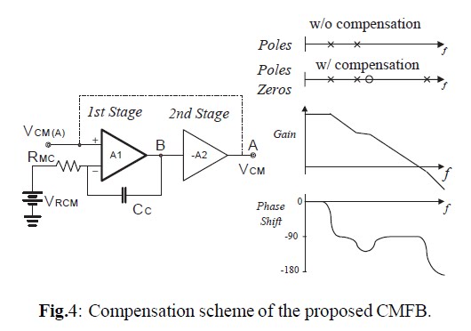
Two high-impedance places, two external nodes (A) and one internal node (B) in Figure 3, introduce two low frequency poles and cause a stability problem. Frequency compensation is achieved by adding MC and CC. With CC shunted to the input and output of the first stage, an extra pole and zero are introduced to attenuate the high frequency gain of the first stage. The gain of the first stage reduces to one for a high-frequency range and causes the CMFB to function as a single-stage CMFB. Accordingly, the proposed CMFB has a large low-frequency gain to minimize VERR and a moderate high-frequency gain to keep the system stable.
Figure 4 shows the compensation scheme of the proposed CMFB.MC and CC (in Figure 3) introduce an extra low-frequency zero to correct the phase shift and an extra high-frequency pole, which has an insignificant effect on the performance. In the proposed CMFB, the common-mode error voltage (VERR) is caused mainly by the transistor mismatch, which is in the mV range.
Figure 4 shows the compensation scheme of the proposed CMFB.MC and CC (in Figure 3) introduce an extra low-frequency zero to correct the phase shift and an extra high-frequency pole, which has an insignificant effect on the performance. In the proposed CMFB, the common-mode error voltage (VERR) is caused mainly by the transistor mismatch, which is in the mV range.
3. Experiment Result
The proposed CMFB has been implemented in a second order continuous-time switched current Σ∆ modulator (Fig. 5) in a 2um CMOS process [9]. The accuracy and stability of the common-mode voltages in the Σ∆ modulator are important since they affect the gain of the Voltage-to-Current Converter (in Figure 5) due to the body effect [9].

The proposed CMFB is designed to accommodate ± 1V differential voltage swing. Figure 6 shows the relationship between VERR and the differential input voltage within±1V. From Figure 6, VERR is less than 0.4mV within the designated differential input voltage range. Here, the mismatch among M1–M4 is ignored. Figure 7 shows an expanded view of VERR over the differential input range within ± 2V.


Figure 8 shows the open-loop transconductance of the proposed CMFB. The performance summary is shown in Table 2. Figure 9 shows a microphotograph of the proposed CMFB circuit. A second-order continuous-time switched-current Σ∆ modulator with the proposed CMFB has been implemented in a 2u CMOS process and achieved 60dB dynamic range with a 50MHz clock.


4. Conclusion
A continuous-time common-mode feedback circuit is presented. The two-stage CMFB structure minimizes the common-mode error voltage without a stability problem. The high output impedance and small common-mode error voltage make it an ideal CMFB, even for a high impedance current-mode system. The proposed CMFB can be easily implemented in any differential mode circuits without modifying differential amplifiers or other circuits in the system. The measured result of the second order continuous-time switched-current Σ∆ modulator has proven the superior performance of the proposed CMFB.
Hernández Caballero Indiana
Asignatura: CAF
Fuente:http://citeseerx.istpsu.edu
No hay comentarios:
Publicar un comentario