jueves, 20 de mayo de 2010

Fully Differential Op Amps Made Easy

1 Introduction

Fully differential op amps may be intimidating to some designers, But op amps began as fully differential components over 50 years ago. Techniques about how to use the fully differential versions have been almost lost over the decades. However, today’s fully differential op amps offer performance advantages unheard of in those first units.
 
This report does not attempt a detailed analysis of op amp theory; reference 1 covers theory well. Instead, this report presents just the facts a designer needs to get started, and some resources for further design assistance. After reading this document, a designer can approach a fully differential op amp design with confidence.
 
2 What Does Fully Differential Mean?
 
Single-ended op amps have two inputs—a positive and negative input—which are understood to be fully differential. They have a single output, which is referenced to system ground.

The op amp has two power supply inputs, which are connected to bipolar power supplies (equal and opposite positive and negative potentials), or a single potential, with a positive supply and a ground connected to the power supply pins. These power supply pins are often omitted from the schematic symbol, when power supply connections are implied elsewhere on the schematic.
 
Fully differential op amps add a second output:

 The output is fully differential—the two outputs are called positive output and negative output—similar terminology to the two inputs. Like the inputs, they are differential. The output voltages are equal, but opposite in polarity (referenced to the common-mode operating point of the circuit).

3 How Is the Second Output Used?

An op amp is used as a closed-loop device. Most designers know how to close the loop on a single-ended op amp:


Whether the single ended op amp is used in an inverting or a noninverting mode, the loop is closed from the output to the inverting input.

3.1 Differential Gain Stages

So, how is the loop closed on a fully differential op amp? If there are two outputs, both of them have to be operated closed loop. Therefore, the equivalent way of closing the loop on a fully differential op amp is:

Two identical feedback loops are required to close the loops for a fully differential op amp. If the loops are not matched, there can be significant second order harmonic distortion. For a fully differential op amp, each feedback loop is an inverting feedback loop. Both polarities of output are available, so terms like inverting and noninverting are meaningless. Instead, think of the single-ended schematics in Figure 3. In both cases, the loop goes from the noninverting output to the inverting input, introducing a 180° phase shift. For the fully differential op amp, the top feedback loop has a 180° phase shift from the noninverting output to the inverting input, and the bottom feedback loop has a 180° phase shift from the inverting output to the noninverting input. Both feedback paths are therefore inverting. There is no noninverting fully differential op amp gain circuit.

The gain of the differential stage is:

3.2 Single-Ended to Differential Conversion

The schematic shown in Figure 4 is a fully differential gain circuit. Fully differential applications, however, are somewhat limited. Very often the fully differential op amp is used to convert a single-ended signal to a differential signal—perhaps to connect to the differential input of an A/D converter.
 

The two configurations shown in Figure 5 are equivalent. At first glance, they look identical, but they are not. The difference is that in the left configuration, the inverting input is used for signal and the noninverting input for reference. In the right configuration, the noninverting input is used for signal and the inverting input for reference. Either one works.

The gain of the single-ended to differential stage is:
The only difference between this configuration and the previous is that one side of the input voltage is referenced to ground. 

The dynamics of the gain are sometimes best described pictorially. Figure 6 shows the relationship between Vin, Vout+, and Vout–.


4 A New Function

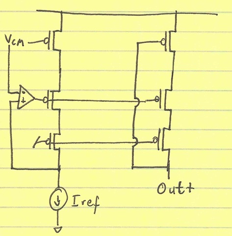
Texas Instruments fully differential op amps have an additional pin, Vocm, which stands for common-mode output voltage (level). The function of this pin can be either an input or an output, because its source is just a voltage divider off the power supply, but it is seldom used as an output. When it is used as an output, it corresponds to the common-mode voltage about which the Vout+ and Vout– outputs swing.

The most common use of the Vocm pin is to set the output common-mode level of the fully differential op amp. This is a very useful function, because it can be used to match the common mode point of a data converter to which the fully differential amplifier is connected. Highprecision/ high-speed data converters often employ differential inputs and provide a reference output.
The schematic of Figure 8 is simplified, and does not show compensation, termination, or decoupling components for clarity. Nevertheless, it shows the basic concept.
 
There are misconceptions associated with the Vocm pin:

* Misconception 1: The Vocm pin can be used as a third input. The Vocm pin is not a third signal input. Texas Instruments continually receives requests to know the bandwidth of the Vocm input. This is not the intended use. The intended use of the Vocm pin is to allow an external voltage to set the common-mode point of the output of the fully differential op amp

* Misconception 2: The Vocm pin can be used to set the dc operating point. Texas Instruments receives many customer inquiries about single supply operation of fully differential op amps, where the customer is attempting to use the Vocm pin to set the half supply reference. This invariably causes the circuit to draw excess current, and it can violate the input common mode range of the device. Proper dc operating point must be set with conventional op amp design techniques. Reference 2 describes the proper way to set the dc operating point of fully differential op amps.

* Misconception 3: The Vocm voltage level, reflected at the output, is affected by the stage gain. The common-mode output voltage is not affected by the values of Rf and Rg. The actual relation governing Vocm is:

The designer can think of Vocm in this way: as Vocm is shifted from zero to higher values, the dc portion of Vout+ and Vout– shifts by the same amount. The differential voltage between the two outputs, however, remains constant—determined by the values of Rf and Rg.
 
The value of Vocm affects the maximum output voltage swing. The maximum output voltag swing happens when Vocm is at zero. Adding 1 Vdc to Vocm decreases the output voltage swing range by one volt. For example, the voltage swing range for THS4131 is 3.7 V, –4.3 V when the supply voltage is ±5 V. This means that the output signal may reach 1.3 V below the upper rail
and 0.7 V above the negative rail.
 
Consider the case when the input signal is 2 VPP, and the gain of the circuit is one:

* If Vocm is zero, the Vout+ and Vout– outputs swing to ±1 Vac, and since the voltage rail is 3.7 Vdc, there is plenty of headroom on both rails, and the design works.

* If Vocm is raised to 3 Vdc, then both outputs attempt to swing between 2 V and 4 V, and alternately hit the positive rail, clipping at 3.7 V.

* Similarly, if Vocm is lowered to –3.5 Vdc, then both outputs attempt to swing between –2.5 V and –4.5 V, and alternately hit the negative rail, clipping at –4.3 V
 
These three cases are combined in Figure 9. 

5 Conclusions
 
Fully Differential op amps, although not a new type of component, are new to most designers. Techniques to use these components are similar to the techniques used to design inverting single-ended op amps. The number of outputs and feedback paths is increased to 2, doubling the number of passive components needed to support a fully differential design. The Vocm pin of the device is a new concept, which facilitates connection to a reference output from a data converter.

Hernández Caballero Indiana
Asignatura: CAF
Fuente:http://focus.ti.com/lit/an/sloa099/sloa099.pdf

martes, 18 de mayo de 2010

A Differential Op-Amp Circuit Collection - Parte IV

5 Audio Applications

5.1 Bridged Output Stages


The presence of simultaneous output polarities from a fully-differential amplifier solves a problem inherent in bridged audio circuits – the time delay caused by taking a single-ended output and running it through a second inverting stage.


The time delay is nonzero, and a degree of cancellation as one peak occurs slightly before the other when the two outputs are combined at the speaker. Worse yet, one output will contain one amplifier’s worth of distortion, while the other has two amplifier’s worth of distortion. Assuming traditional methods of adding random noise, that is a 41.4% noise increase in one output with respect to the other, power output stages are usually somewhat noisy, so this noise increase will probably be audible.

A fully-differential op-amp will not have completely symmetrical outputs. There will still be a finite delay, but the delay is orders of magnitude less than that of the traditional circuit.


This technique increases component count and expense. Therefore, it will probably be more appropriate in high end products. Most fully-differential op-amps are high-speed devices, and have excellent noise response when used in the audio range.

5.2 Stereo Width Control

Fully-differential amplifiers can be used to create an amplitude cancellation circuit that will remove audio content that is present in both channels.


The output mixers (U2 and U4) are presented with an inverted version of the input signal on one input (through R6 and R14), and a variable amount of out-of-phase signal from the other channel.

When the ganged pot (R5) is at the center position, equal amounts of inverted and noninverted signal cancel each other, for a net output of zero on the other input of the output mixers (through R7 and R13).

At one extreme of the pot (top in this schematic), the output of each channel is the sum of the left and right channel input audio, or monaural. At the other extreme, the output of each mixer is devoid of any content from the other channel – canceling anything common between them.

This application differs from previous implementations by utilizing fully-differential op-amps to simultaneously generate inverted and noninverted versions of the input signal. The usual method of doing this is to generate an inverted version of the input signal from the output of a buffer amp. The inverted waveform, therefore, is subject to two op-amp delays as opposed to one delay for the non-inverted waveform. The inverted waveform, therefore, has some phase delay which limits the ultimate width possible from the circuit. By utilizing a fully-differential opamp, a near perfect inverted waveform is available for cancellation with the other channel.

6 Summary

Fully-differential amplifiers are based on the technology of the original tube-based op-amps of more than 50 years ago. As such, they require design techniques that are new to most designers. The performance increase afforded by fully differential op-amps more than outweigh the slight additional expense of more passive components. Driving of fully differential A/D converters, data filtering for DSL and other digital communication systems, and audio applications are just a few ways that these devices can be used in a system to deliver performance that is superior to single-ended design techniques.


Hernández Caballero Indiana
Asignatura: CAF
Fuente: http://focus.ti.com/lit/an/sloa064/sloa064.pdf

A Differential Op-Amp Circuit Collection - Parte III

4 Driving Differential Input Data Converters

Most high-resolution, high-accuracy data converters utilize differential inputs instead of singleended inputs. There are a number of strategies for driving these converters from single-ended inputs.
In Figure 14, one amplifier is used in a noninverting configuration to drive a transformer primary. The secondary of the transformer is center tapped to provide a common-mode connection point for the A/D converter Vref output.

 Gain can be added to the secondary side of the transformer. In Figure 15, two single-ended op amps have been configured as inverting gain stages to drive the A/D Inputs. The non-inverting input inputs are connected to the transformer center tap and A/D Vref output.
Figure 16 shows how single-ended amplifiers can be used as noninverting buffers to drive the input of an A/D. The advantage of this technique is that the unity gain buffers have exact gains, so the system will be balanced.

Transformer interfacing methods all have one major disadvantage:
 
* The circuit does not include dc in the frequency response. By definition, the transformer isolates dc and limits the ac response of the circuit.

If the response of the system must include dc, even for calibration purposes, a transformer is a serious limitation. A transformer is not strictly necessary. Two single-ended amplifiers can be used to drive an A/D converter without a transformer:
Although all of the methods can be employed, the most preferable method is the use a fully differential op-amp:
A designer should be aware of the characteristics of the reference output from the A/D converter. It may have limited drive capability, and / or have relatively high output impedance. A high-output impedance means that the common mode signal is susceptible to noise pickup. In these cases, it may be wise to filter and/or buffer the A/D reference output:

Some A/D converters have two reference outputs instead of one. When this is the case, the designer must sum these outputs together to create a single signal as shown in Figure 20:


Hernández Caballero Indiana
Asignatura: CAF
Fuente: http://focus.ti.com/lit/an/sloa064/sloa064.pdf

A Differential Op-Amp Circuit Collection - Parte II


3 FILTER CIRCUITS

Filtering is done to eliminate unwanted content in audio, among other things. Differential filters that do the same job to differential signals as their single-ended cousins do to single-ended signals can be applied.

For differential filter implementations, the components are simply mirror imaged for each feedback loop. The components in the top feedback loop are designated A, and those in the bottom feedback loop are designated B. For clarity decoupling components are not shown in the following schematics. Proper operation of high-speed op-amps requires proper decoupling techniques. That does not mean a shotgun approach of using inexpensive 0.1-ìF capacitors. Decoupling component selection should be based on the frequencies that need to be rejected, and the characteristics of the capacitors used at those frequencies.

3.1 Single Pole Filters

Single pole filters are the simplest filters to implement with single-ended op-amps, and the same holds true with fully-differential amplifiers. A low pass filter can be formed by placing a capacitor in the feedback loop of a gain stage, in a manner similar to single-ended op-amps:


A high pass filter can be formed by placing a capacitor in series with an inverting gain stage as shown in Figure 4:


3.2 Double Pole Filters

Many double pole filter topologies incorporate positive and negative feedback, and therefore have no differential implementation. Others employ only negative feedback, but use the noninverting input for signal input, and also have no differential implementation. This limits the number of options for designers, because both feedback paths must return to an input.

The good news, however, is that there are topologies available to form differential low pass, high pass, bandpass, and notch filters. However, the designer might have to use an unfamiliar topology or more op-amps than would have been required for a single-ended circuit.

3.2.1 Multiple Feedback Filters

MFB filter topology is the simplest topology that will support fully-differential filters. Unfortunately, the MFB topology is a bit hard to work with, but component ratios are shown for common unity gain filters. 

Reference 5 describes the MFB topology in detail.


There is no reason why the feedback paths have to be identical. A bandpass filter can be formed by using nonsymmetrical feedback pathways (one low pass and one high pass). Figure 7 shows a bandpass filter that passes the range of human speech (300 Hz to 3 kHz).


3.2.2 Akerberg Mossberg Filter

Akerberg Mossberg filter topology is a double pole topology that is available in low pass, high pass, band pass, and notch. The single ended implementation of this filter topology has an additional op-amp to invert the output of the first op-amp. That inversion in inherent in the fullydifferential op-amp, and therefore is taken directly off the first stage. This reduces the total number of op-amps required to 2:


3.2.3 Biquad Filter

Biquad filter topology is a double pole topology that is available in low pass, high pass, band pass, and notch. The highpass and notch versions, however, require additional op-amps, and therefore this topology is not optimum for them. The single-ended implementation of this filter topology has an additional op-amp to invert the output of the first op-amp. That inversion is inherent in the fully-differential op-amp, and therefore is taken directly off the first stage. This reduces the total number of op-amps required to 2:


Hernández Caballero Indiana
Asignatura: CAF
Fuente: http://focus.ti.com/lit/an/sloa064/sloa064.pdf
 

A Differential Op-Amp Circuit Collection - Parte I


1 INTRODUCTION

The idea of fully-differential op-amps is not new. The first commercial op-amp, the K2-W, utilized two dual section tubes (4 active circuit elements) to implement an op-amp with differential inputs and outputs. It required a 300 Vdc power supply, dissipating 4.5 W of power, had a corner frequency of 1 Hz, and a gain bandwidth product of 1 MHz(1).

In an era of discrete tube or transistor op-amp modules, any potential advantage to be gained from fully-differential circuitry was masked by primitive op-amp module performance. Fully-differential output op-amps were abandoned in favor of single ended op-amps. Fully-differential op-amps were all but forgotten, even when IC technology was developed. The main reason appears to be the simplicity of using single ended op-amps. The number of passive components required to support a fully-differential circuit is approximately double that of a single-ended circuit. The thinking may have been “Why double the number of passive components when there is nothing to be gained?”

Almost 50 years later, IC processing has matured to the point that fully-differential op-amps are possible that offer significant advantage over their single-ended cousins. The advantages of differential logic have been exploited for 2 decades. More recently, advanced high-speed A/D converters have adopted differential inputs. Single-ended op-amps require a problematic transformer to interface to these differential input A/D converters. This is the application that spurred the development of fully-differential op-amps. An op-amp with differential outputs, however, has far more uses than one application.

2 BASIC CIRCUITS

The easiest way to construct fully-differential circuits is to think of the inverting op-amp feedback topology. In fully-differential op-amp circuits, there are two inverting feedback paths:

•    Inverting input to noninverting output

•    Noninverting input to inverting output

Both feedback paths must be closed in order for the fully-differential op-amp to operate properly.

When a gain is specified in the following sections, it is a differential gain – that is the gain at VOUT+ with a return of VOUT-. Another way of thinking of differential outputs is that each signal is the return path for the other.

2.1 A New Pin

Fully-differential op-amps have an extra input pin (VOCM). The purpose of this pin is to provide a place to input a potentially noisy signal that will appear simultaneously on both inputs – i.e. common mode noise. The fully-differential op-amp can then reject the common mode noise.

The VOCM pin can be connected to a data converter reference voltage pin to achieve tight tracking between the op-amp common mode voltage and the data converter common mode voltage. In this application, the data converter also provides a free dc level conversion for single supply circuits. The common mode voltage of the data converter is also the dc operating point of the single-supply circuit. The designer should take care, however, that the dc operating point of the circuit is within the common mode range of the op-amp + and – inputs. This can most easily be achieved by summing a dc level into the inputs equal or close to the common mode voltage.

2.2 Gain

A gain stage is a basic op-amp circuit. Nothing has really changed from the single-ended design, except that two feedback pathways have been closed. The differential gain is still Rf /Rin a familiar concept to analog designers.

This circuit can be converted to a single-ended input by connecting either of the signal inputs to ground. The gain equation remains unchanged, because the gain is the differential gain.


2.3 Instrumentation

An instrumentation amplifier can be constructed from two single-ended amplifiers and a fully-differential amplifier as shown in Figure 2. Both polarities of the output signal are available, of course, and there is no ground dependence.


Hernández Caballero Indiana
Asignatura: CAF
Fuente:http://focus.ti.com/lit/an/sloa064/sloa064.pd
f

lunes, 17 de mayo de 2010

A compact common-mode feedback loop | using a PMOS triode device for CMFB


One of the defining traits of analog CMOS designers is the ability to implement a common-mode feedback (CMFB) loop. When the input devices on a differential pair are all NMOS (or NPN), and the loads are either inductors or resistors, a common-mode feedback loop is unnecessary, because the output resistance of the differential pair is weighted down by the low resistance of the inductor or resistors.

However, when one has a high-impedance trans-conductor (NMOS or PMOS) loaded with a high-impedance current source (PMOS or NMOS), a common-mode feedback loop becomes necessary. Even small differences between the bias current of the trans-conductor and the bias current of the load can induce large swings in voltage when multiplied by the high resistance of the output node.

This post presents a very simple and very effective common-mode feedback method.

Introduction

In a previous post, I detailed what essentially amounts to a common-mode feedback circuit. It was shown as a level-shifter, but at its core, it sense the common-mode (average between the differential outputs) and adjusted it to a reference value. If there is interest, I can detail how to apply that topology in a differential pair to create a common mode feedback loop; just post a request in the comments.

The difficulty with that approach is that it places the common-mode feedback loop directly on the output branches. Precision in the common-mode requires high gain the common-mode feedback loop. In the case where there is a capacitor load on the output branches (most of the time), this high gain causes a stability concern. The bandwidth of the gain must be lowered for stability.

There is a another way to accomplish common-mode feedback. (It has been published in a journal or conference article in the past. I will give a reference when I have access to the IEEE database.) The benefit of this approach is that it separates the precision of the common-mode voltage from stability concerns.

I will consider the case where we have an NMOS-input diff pair with PMOS loads. The common-mode feedback involves placing an extra set of PMOS devices that are connected together. These extra devices are biased in triode. The reference (diode-connected) branch should also have this triode device:


I have excluded the input NMOS diff-pair because it would clutter the sketch.

This common-mode feedback works by changing the source voltage on the PMOS current sources in proportion to the output common-mode. The connection between the two triode devices does an averaging of the two PMOS-source voltages.

Analysis

Since we are just considering the common-mode effect, we can assume a zero differential and therefore the two output branches (negative and positive) have exactly the same (in terms of both node voltages and branch currents). As a result, we don’t need to draw both branches each time. We can simply draw one branch (pick one)—or we can consider a single (equivalent) branch that is the average of the two differential branches:


Note that the reference branch has a triode PMOS device that is connected to the desired common mode, VCM. If the output branch is loaded with Iref, then the voltages will be exactly the same. Let’s now consider what happens when the output is not loaded in Iref, but something a little smaller. I’ll denote with arrows the direction that different values take. For example, if the load current has gone down:


You’ll also note that I’ve done away with the cascode device as it does not affect the analysis. The load current going down will cause the output voltage to go up:


This in turn will cause the resistance of the triode PMOS to go up shown now as a voltage-controlled resistor Rx:


This increased resistance then causes the source of the PMOS to go down in voltage Vx:


The source Vx of the PMOS going down in voltage reduces the |VGS| of the PMOS device, thus reducing the voltage it puts out. Thus its output current Io is reduced:


Io being reduced then causes the output voltage Vo to go down:


Vo going up thus negates the initial effect of Vo going up, completing a negative feedback loop. What has happened is that the PMOS side has adjusted its current to match the NMOS side, thus leaving the output voltage intact but changing the current through the branch.

One more thing

The astute reader will notice that all this negative feedback, in the end, only makes the output current Vo equal to the gate voltage on the diode connected device. It does not actually place the output voltage at the desired common-mode voltage. To do so, we need to add one more op-amp to the reference branch:


You might feel cheated at this point to learn that you still need a differential amplifier that senses and adjusts common-mode. However, the beauty of the system is that this reference branch is not operating directly on the output branch. If there are capacitors on the output branch, they are designed independently of the stability of the reference branch. As a result, one can place extremely high gain on it to get a very precise common-mode voltage without worrying about stability.

Conclusion

The output branches of an OTA already have a high gain from the gates of the current-source loads to its output. As a result, a separate high-gain stage is not necessary. The main benefit of the triode-based CMFB loop is its ability to average the common mode of two differential branches without requiring a separate summing amplifier or a resistor sense, all in a low-gain highly-stable configuration

The triode-based CMFB allows one to create a wide-band, stable common-mode feedback loop on the output branches to cancel the dynamic common mode perturbations. A separate loop handles precise bias of the current source devices to target a reference common mode. This separate loop can be made arbitrarily high gain while maintaining stability. However, this separation can also be achieved with a more typical common-mode feedback sensing amplifier configuration. (If there is interest in this topic, please post in the comments.)

The main downfall of the triode-based CMFB is that some albeit small amount of voltage is dropped across the triode devices. This drop eats up some headroom, but more importantly, it robs some voltage drop from the current source/cascode devices, thus generating more differential noise in the current sources.

Generalization

This current adjustment to maintain a voltage is what every good common-mode feedback loop does—and it is also why the common-mode resistance of the system is low. Deviations in current result in very little voltage swing; so, the V/I ratio is low. At the same time, any differential current does not cause the common-mode feedback loop to react; the CMFB only senses common-mode. Thus, large differential voltage swings result from changes in differential current. Common-mode feedback loops allow for high differential output resistance with low common-mode output resistance.


Hernández Caballero Indiana
Asignatura: CAF
Fuente:
http://www.circuitdesign.info/blog/2008/10/a-compact-common-mode-feedback-loop-using-a-pmos-triode-device-for-cmfb/