viernes, 25 de junio de 2010

Common-Mode Control Techniques for Low Voltage Continuous-Time Analog Signal Processors


Abstract-Fully-Differential (FD) circuits are unavoidable under low voltage power supply conditions. To properly operate FD circuits the use of common-mode feedback is compulsory. The conceptual approach to implement the common-mode feedback circuits is introduced. Furthermore, the use of common-mode feedforward techniques to enhance the common-mode rejection ratio is introduced. It is demonstrated that the simultaneous application of common-mode feedback and common-mode feedforward yields optimal performance with only an additional small overhead cost.

I. INTRODUCTION


The rapid size reduction of CMOS technologies is limiting the maximum power supply voltage that integrated circuits (IC) can sustain, and this trend [1] will continue. In a digital IC, as devices dimensions shrink, more and more devices can be fabricated on the same die, the parasitic capacitances also tend to decrease, and current density increases. The combined effect is a reduction of the propagation delay, which allows higher throughput and clock rates for digital circuits. The performance of digital circuits improves with the size reduction of the technology. Unfortunately, from a general point of view, technology scaling has a negative impact on the performance of analog integrated circuits. Therefore, scaling degrades the intrinsic gain of the devices and, what is even more critical, the very limited voltage room available reduces the circuit dynamic range (DR) with respect to the DR counterparts for higher supply voltages. Therefore, in such low supply voltage (LV) conditions, analog circuits require larger input/output voltage signal swings, enhanced linearity, and larger rejection to undesired signals, to keep a similar performance with respect to the operation at higher supply voltages. Many analog design issues, which were unimportant only a decade ago, are now of vital importance and new circuit topologies and design strategies must be investigated for supply voltages in the order of one MOS transistor threshold voltage [2]. In this papers, the type and control of the common-mode (CM) component of (differential) signals in LV analog signal processors, is presented. Traditionally, common-mode feedback (CMFB) techniques have been applied for the control of the output CM component in (FD) circuits. However, most of the conventional techniques are not valid for very LV applications and hence, alternative solutions are needed. The merging of common-mode feedforward and common-mode feedback techniques to enhance circuit performance will be introduced.


II COMMON-MODE FEEDBACK PRINCIPLES


One of the most useful building blocks in analog signal processors is the operational amplifier (Op Amp) or operational transconductance amplifier (OTA). For small size technologies the power supply is limited, but the output signal swing still needs to be large. One solution to increase the output signal is to use fully differential amplifiers. That is both differential input and differential output. Fig. 1 illustrates the conceptual architecture of the use of common-mode feedback. The basic idea is to first monitor the common-mode signal (that is the sum of the output signals) and then compare the common mode signal with a reference voltage, which usually is 0 volts. Thus a correction signal is generated and applied to the fully differential amplifier, such that eventually the correction signal becomes near to zero. The correction signal is the difference between the common-mode signal and the reference voltage. Fig. 2 illustrates an actual implementation of the conceptual architecture of Fig. 1. Fig. 2(a) and (b) illustrate the block and transistor level representation. The two stage differential amplifier has its two outputs connected to two simple differential amplifiers (M21-M24). The outputs of the simple amplifiers are added (in M25) and the corresponding output current is applied to the tail current (M5). The sensing of the output signals can be done in voltage as shown before, but it can be carried out in current. This principle is illustrated in Fig. 3. The amplifier is a transconductance amplifier. This transconductance amplifier consists of a differential pair and two current-mirrors. The common-mode level sensing circuit is applied to the sense amplifier where is compared with a reference current. The output of this CM sense amplifier is then injected to output bias current of the FD amplifier.

The use of common-mode feedback has as objective to: i) cancel the common-mode output signals; ii) fix the DC operating point at the output that maximizes the differential voltage gain. In addition the use of common-mode feedback should reduce the output noise. The actual implementation of the common-mode feedback is not trivial. Several design issues need to be taken into consideration to provide an implementation with the desired specifications and performance. Among them we need to minimize the loading effects of the amplifier when is connected to the sensing amplifier. Stability of the amplifier with feedback must be well defined. Another even more critical issue is the bandwidth of the loops associated with the differential-mode and the common-mode loops. These loop bandwidths should be of the same order to yield a good commonmode rejection ratio in the frequency range of interest. The DC gain of the CMFB loop must be large enough to keep an accurate control the CM component. If not, an asymmetrical swing occurs which entails a loss in the DR. The gain-bandwidth product of the CMFB loop (LGBWCM) should be at least equal to the gain-bandwidth product of the DM loop (LGBWDM) counterpart. We can consider common-mode feedback at the input and output port. Thus if LGBWCM,o < LGBWDM, the system does not perform as a fully-balanced systems in the range of frequencies comprised between LGBWCM,o and LGBWDM; while if LGBWCM,i < LGBWDM occurs, the amplifier does not operate properly since the input CM voltage can be out of the amplifier input CMR in the frequency band comprised between LGBWCM,i and LGBWDM. The CMFB loop must only act over CM voltage signal, while does not affect to any DM voltage signal. If this not occurs, harmonic distortion by the CMFB loop is induced in the signal.

III COMMON-MODE-FEEDFORWARD TECHNIQUES

The use of common-mode Feedforward (CMFF) is very desirable; however note that using only CMFF is not sufficient. CMFF can help to reduce drastically the output common-mode signals, but it cannot help to stabilize the DC output operating bias. The conceptual representation of the CMFF is shown in Fig. 4(a). In the case of multiple cascade amplifiers we can make clever use of CMFF as shown in Fig. 4(b). Note that the common-mode feedforward detector is part of the amplifier; also note that the detection is not done in the amplifier itself but in the next one in the cascade stages. Then a simple feedback is implemented from say amplifier 2 to amplifier 1. One potential transistor level implementation [10] is shown in Fig. 5. Observe in this figure the symmetry and balance of the topology that yields optimal performance as shown later.


IV AN EXAMPLE OF CMFB AND CMFF TECHNIQUES

In this example we show the effect of the CMRR for three different cases. That is a) CMFF only, b) CMFB only, c) CMFB + CMFF. Fig. 6 shows how the combination of the two common-mode techniques yields around 80 dB. Furthermore, the linearity of the amplifier is improved by using both common-mode techniques. Fig. 7 shows that we can obtain up 1.2 peak to peak differential input with less than 1% THD for a 3.3V power supply.

V CONCLUSIONS

A brief introduction to common-mode feedback concepts has been introduced. The key issue in this paper is the strategic use of jointly of the common-mode feedforward and common-mode feedback yielding optimal results for common-mode rejection ratio as well as an improved linearity. More details about LV amplifiers common-mode feedback techniques are available elsewhere.


Hernández Caballero Indiana
Asignatura: CAF
Fuente:http://www.emo.org.tr/ekler/bc10d8a74dbafbf_ek.pdf

It's not just 50 ohms: Some termination tips for differential and single-ended amplifiers


Termination - the term brings to mind different values of resistance to different specialties in electronics. RF designers think about 50 ohm, video designers 75 ohm, audio and telecommunication designers 600 ohm - there are many possibilities. All of these termination resistor values have a common purpose - they match impedances in the circuit and therefore attenuate reflections that would otherwise cause problems in the system.
This article will focus on 50-ohm terminations - but this has more to do with the test equipment available in the author's lab than a preference for RF applications. The techniques established here are applicable to any value of termination resistor, because the electrical laws governing them are universally applicable to other resistance values.
For every input termination resistor, there needs to be a companion series-matching resistor in the source. A laboratory signal source will be assumed. Laboratory sources can be thought of as an ideal voltage source (zero ohm output impedance) in series with a 50 ohm resistor. This resistor is shown as Rs in the schematics below. Laboratory sources assume a 50 ohm termination in the circuit that is driven, and take it into account when generating their display.
For example, a laboratory source is set to 1 Vpp. An ideal source (internal to the instrument and inaccessible to the user) produces a 2 Vpp output. This 2 Vpp output is applied to the internal 50 ohm series-matching resistor. If the source is monitored with a high impedance-measuring instrument -V an oscilloscope with a 1 M-ohm input, for example, it would produce very nearly 2 Vpp - even though the output indicator on the instrument indicates 1 Vpp. When the same source is monitored with an instrument that has a 50 ohm input, the output would be 1 Vpp because Rs and Rt produce a 2:1 voltage divider at the circuit input.
It is very important to realize that the only voltage available to the instrument user is the voltage at its output connector (after the 50 ohm source resistor). Instrument accuracy is only as good as its internal accuracy, as modified by the input termination resistor of the circuit.
It is worth a brief mention that 50 ohm is not a standard one percent resistor value. The closest standard value is 49.9 ohm, and this value has been used in the examples below.
Four cases will be covered in this article: Inverting Stage attenuators Non inverting stage attenuators Single-ended to fully differential stages Differential to fully differential stages
Single-Ended Op Amps
Single-ended op amps are a mature technology - therefore some of what is presented here may be a review. The inverting case, however, is subtle and needs explanation. Inverting Stage Attenuators
Consider the circuit of represented in Figure 1. It assumes a laboratory source as described above. Most designers assume that the 49.9 ohm termination resistor, combined with resistors Rg and Rf will guarantee a gain of 1 - but wait! The real story is a little more complicated.
 Figure 1. Inverting Gain Stage
Assume that the signal source is a laboratory source set to 1 VPP. Both Rg and Rt affect the level of voltage applied to the circuit. The function generator indicates a level of plus-minus 0.5 V (1 VPP) - while only plus-minus 0.484 V (0.968 VPP) is applied to the board. The user might wonder, "what happened - where did the rest of the voltage (plus-minus 0.016 V) go"?
There are two ways of looking at this problem:
From the function generator side. The function generator contains a 50 source resistor. The EVM contains a 49.9 ohm termination resistor, and therefore the output of the function generator will see (approximately) a 2:1 voltage divider. The function generator anticipates this, and scales its output accordingly.
In the inverting configuration, however, the inverting input presents a ground potential to the gain resistor Rg. This is because the ideal op amp model forces both inputs to the same voltage potential. The non-inverting input is connected to ground, and therefore the inverting input will also be at ground. The resulting impedance resistance for the stage will therefore be equal to the termination resistor in parallel to Rg, in this case 750 ohm. Therefore, the instrument output is actually:
This can also be viewed as the Thevenin equivalent voltage looking into the source at Rt.
From the circuit side. The Thevenin equivalent resistance of the circuit plus the source - looking towards the source from the inverting input of the op amp is:

Therefore, the inverting gain on a 0.5 Vpeak ideal voltage source (assumed to be embedded in the function generator) is:
The two results are equivalent.
Non-Inverting Stage Operation
The circuit of Figure 2 contains a 50 ohm terminated input (Rt), and gain setting resistors. Because Rt does not appear in parallel with Rg as in the inverting case, the gain calculation is much simpler - and the termination resistor does not affect the gain expression that the designer is probably familiar with: 

Figure 2. Non-Inverting Gain Stage Figure
Fully Differential Op Amps
Fully differential op amps present some special challenges for terminated operation, because they should have two balanced feedback loops for symmetrical operation. Termination presents some special problems for this requirement.
Two cases will be discussed. One is single ended signal input, the other fully differential signal input.
Single-Ended to Fully Differential Conversion
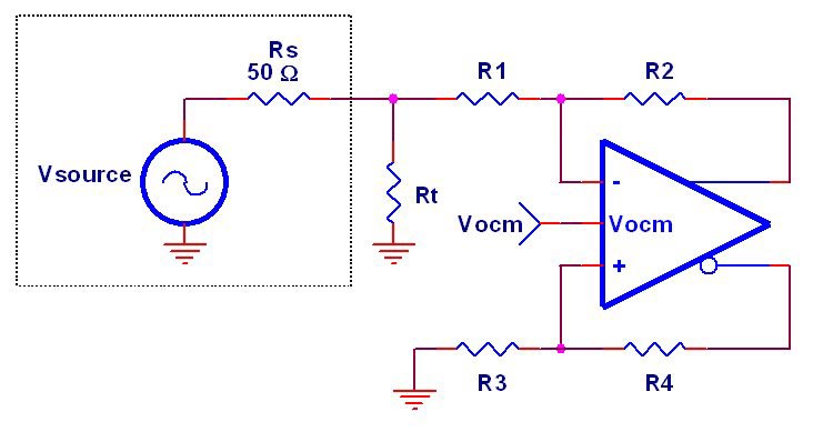
Termination is applied to one of the two inputs - the other input is grounded as shown in Figure 3. This automatically creates an imbalance in the two feedback loops. Some of the reasons are described in the section above - all of that analysis applies to the bottom feedback path. 
Figure 3. Single-Ended to Fully Differential
The overall effect, of course, is to place 25 more ohms on the bottom feedback path than on the top (Rs || Rt + R3). This means that the gain on the bottom feedback path is less than that of the top. So, 25 ohms must also be added to R1. But this changes the gain of the entire circuit to less than 1, so both R1 and R3 must both be decreased to boost the gain. This could go one and on - the design is an interactive process. To simplify this task for designers, Texas Instruments provides an on-line calculator on its web site. This tool can be accessed either through the Analog and Mixed-Signal Knowledgebase, or through the Engineering Design Utilities section on the Analog and Mixed Signal portion of the TI web site. 
Figure 4 shows a screen shot of the fully differential amplifier component calculator.
The fully differential component calculator has six panes. Data entry is primarily made in the upper left pane, although the bottom middle pane contains some secondary entry fields.
The top middle pane contains the schematic for a terminated single-ended to fully differential conversion. Design equations are shown in the upper right hand pane. The equations for RR3,R4 and Rt are interrelated through the ''A'' parameter. The tool will make a preliminary calculation to get close to the correct values, and then it will refine the calculation and ''goal seek'' to the final value. The execution time depends on the step size used in the goal seeking calculation, and therefore selecting ''E96'' resistor values will execute much faster than ''Exact'' values. The designer should be patient, because execution times of several seconds or longer are possible, especially if gain is changed radically when ''Exact Values'' is selected. The designer selects the desired gain and the impedance of the signal source (default value of 50 ohms). The designer then has the option of selecting a seed value for either R3 or R4 (but not both). If the designer attempts to select both, only the last value entered will be used for calculation.
Almost without exception, the designer should initially try to select the value of R4, because it is often specified on the data sheet. The designer should experiment with R3 only if the recommended value of R4 does not yield an acceptable design (the tool has internal limits set to resistor values that make sense for real designs).
When the designer selects ''Calculate Values,'' the tool will calculate resistor values in the bottom left pane and circuit simulation results in the bottom right pane. If the designer wishes, the power and input voltages can be changed in the bottom middle pane, and these will affect the simulation results in the bottom right.
Note that this tool provides dc operating point only - it does not give ac simulation. Nevertheless, it will save the designer a lot of grief trying to do it the ''brute force'' method.
The implementation of Figure 5 is completely equivalent to that of Figure 3, it does not matter which input is used for the signal. 
Figure 5. Alternative Single-Ended to Fully Differential Conversion
Fully-Differential In/Fully-Differential Out
Consider the circuit of Figure 6. In this configuration, input termination (resistor R1), is used to terminate a fully differential input.
Fully differential gain for the un-terminated case is determined by the relationship:
 Where Rf is R3 in the top feedback loop and R6 in the bottom, and Rg is R2 on top and R5 on the bottom.
The designer should recognize the gain expression as being very close to the expression for the single-ended inverting stage (but without the negative sign). There is no negative sign because it is meaningless when both polarities of output are simultaneously available. 
Figure 6. Fully Differential Operation
When a termination resistor is used, it affects the gain in a manner similar to the single-ended cases. In this case, however, the effect is not as intuitive.
Figure 7 shows the input of a differential stage as an ideal voltage source, with its characteristic 50 ohm source impedance split in two parts, between a "phantom ground". The termination resistor is also shown in two parts between the same phantom ground. The end result is the two 25 ohm resistors above the phantom ground appearing as a single 12.5 ohm resistor (the parallel combination). This 12.5 ohm resistance appears in series with the top Rg, changing the gain. Similarly, the two 25 ohm resistors below the phantom ground add to the bottom Rg, changing the gain and balancing the top gain.
Figure 7. Fully Differential Operation
The gain of the fully differential stage, therefore, is:
For the circuit of Figure 6, the differential gain is:

Changing the gain is much more straightforward than in the previous case, because equal changes made to the top and bottom feedback loop simultaneously are inherently symmetrical.
Output Series Resistor Matching
The circuits shown above can also be considered to be voltage sources. The output impedance of most op amp circuits (operated in a closed loop) is low enough that it can be considered to be zero. Therefore, it is a good approximation to consider closed loop op amp to be an ideal voltage source.
The reader is reminded that in the discussion above, an ideal voltage source is assumed to be at the heart of a laboratory voltage source. Therefore, by extrapolation, the reader hopefully sees how to cascade terminated stages - by adding 50 ohms in series with the op amp output to create a 50 ohm "source" for the subsequent stage.
This is often the case in RF design, where each stage has 50 ohm input and output. If the circuits above drive a 50 ohm load, they need a 50 ohm resistor in series with the op amp output. This will, of course, create a 2:1 voltage divider (-6 dB) with the termination resistor in the subsequent stage. This has to be taken into account in the design of overall system gain. It takes 6 dB of stage gain to compensate for a 2:1 voltage divider. The -20 dB per decade slope of the open loop response of a typical voltage feedback op amp, combined with 6 dB of gain forces a designer to choose a part with approximately four times the bandwidth that would be required for a unity gain stage.
The proper application of termination is a powerful way of suppressing reflections in high-speed circuits. It comes with a price; however, it introduces voltage dividers that attenuate the signal. Stage gain has to be increased to compensate - and that often times dictates a much higher bandwidth part to accommodate the additional gain required.
Termination can introduce subtle gain errors into a circuit if it effects are not properly taken into account. The rules governing termination are simple - Ohm's law, the voltage divider law, and the superposition principle - therefore it is not asking a great deal from analog designers to do the calculations. The only exception is the case of termination a single-ended to fully differential conversion, and Texas Instruments has provided a utility to simplify the task.

Hernández Caballero Indiana
Asignatura: CAF
Fuente:http://www.planetanalog.com/story/OEG20020724S0082

jueves, 24 de junio de 2010

Texas Instruments introduces a differential amplifier family


Texas Instruments has introduced a fully differential amplifier family that drives high accuracy data conversion across single and multi-channel SAR (successive approximation register) and delta-sigma ADCs (analogue-to-digital converters) in a wide range of applications including industrial, medical and audio. The THS4521, THS4522 and THS4524 provide good performance to power ratio, making the devices suitable for applications requiring high resolution and precision with high dynamic range, such as pressure and flow meters, seismic equipment and electrocardiogram machines, as well as battery-operated devices and other applications with sensitive power budgets. This product family provides an alternative that reduces the number of amplifiers to save board space and alleviates amplifier and circuit matching concerns while minimising power consumption.

The devices consume low quiescent current of 1.14mA per channel and less power down current of 20uA. The family increases the bandwidth by more than 30%, providing 145MHz and 490V/μs slew rate to buffer and amplify signals without increasing the system power consumption. It improves dynamic range/sensitivity by 44% with an input voltage noise of 4.6nV/rtHz to minimise distortion. The output common mode control allows easy DC coupling, while negative rail input and rail-to-rail output capability simplifies design and shortens development time. The device offers power supply flexibility by accepting single supply of +3 to +5V or dual supply of ±1.5 to ±2.5V. The amplifier reduces board space with single, dual and quad configuration options.

The amplifier devices enable customers to drive differential ADCs, including the company's ADS8317 16bit, 250ksamples/s SAR converter and ADS1278 24bit, 128ksamples/s delta-sigma converter and achieve specified data sheet performance levels. For instance, using the THS4521 to buffer the ADS1278, at 10kHz input achieves 102dB SNR (signal-to-noise ratio) and 110dBc SFDR (spurious free dynamic range) with low quiescent current, which reduces system power consumption.

Hernández Caballero Indiana
Asignatura: CAF
Fuente:http://www.epn-online.com/page/new112261/texas-instruments-introduces-a-differential-amplifier-family.html

Fully differential amplifier


A fully differential amplifier , usually referred to as an 'FDA ' for brevity, is a DC- coupled high-gain electronic voltage amplifier with differential inputs and differential outputs. In its ordinary usage, the output of the FDA is controlled by two feedback paths which, because of the amplifier's high gain, almost completely determines the output voltage for any given input.


The ideal FDA

For any input voltages the ideal  FDA has infinite open-loop gain, infinite bandwidth, infinite input impedances resulting in zero input currents, infinite slew rate, zero output impedance and zero noise.

A Real FDA can only approximate this ideal, and the actual parameters are subject to drift over time and with changes in temperature, input conditions, etc. Modern integrated FET or MOSFET FDAs approximate more closely to these ideals than bipolar ICs where large signals must be handled at room temperature over a limited bandwidth; input impedance, in particular, is much higher, although the bipolar FDA usually exhibit superior (i.e., lower) input offset drift and noise characteristics.

Where the limitations of real devices can be ignored, an FDA can be viewed as a Black Box with gain; circuit function and parameters are determined by feedback, usually negative. An FDA as implemented in practice is moderately complex integrated circuit

Limitations of real FDAs

DC imperfections

    *  Finite gain — the effect is most pronounced when the overall design attempts to achieve gain close to the inherent gain of the FDA.
    *  Finite input resistance — this puts an upper bound on the resistances in the feedback circuit.
   *  Nonzero output resistance — important for low resistance loads. Except for very small voltage output, power considerations usually come into play first. (Output impedance is inversely proportional to the idle current in the output stage — very low idle current results in very high output impedance.)
    *  Input bias current — a small amount of current (typically ~10 nA for bipolar FDAs, or picoamperes for CMOS designs) flows into the inputs. This current is mismatched slightly between the inverting and non-inverting inputs (there is an input offset current). This effect is usually important only for very low power circuits.
    *  Input offset voltage — the FDA will produce an output even when the input pins are at exactly the same voltage. For circuits which require precise DC operation, this effect must be compensated for.
    *  Common mode gain — A perfect operational amplifier amplifies only the voltage difference between its two inputs, completely rejecting all voltages that are common to both. However, the differential input stage of an FDA is never perfect, leading to the amplification of these identical voltages to some degree. The standard measure of this defect is called the common-mode rejection ratio (denoted, CMRR). Minimization of common mode gain is usually important in non-inverting amplifiers (described below) that operate at high amplification.
    *  Temperature effects — all parameters change with temperature. Temperature drift of the input offset voltage is especially important.

AC imperfections

    *  Finite bandwidth — all amplifiers have a finite bandwidth. This is because FDAs use internal frequency compensation to increase the phase margin.
    *  Input capacitance — most important for high frequency operation because it further reduces the open loop bandwidth of the amplifier.
    *  Common mode gain — See DC imperfections, above.
    *  Noise - all real electronic components (except superconductor) generate noise. You can find devices with 0.8 to several hundreds nv/rtHz noise performance.

Nonlinear imperfections

    * Saturation — output voltage is limited to a peak value, usually slightly less than the power supply voltage. Saturation occurs when the differential input voltage is too high for the op-amp's gain, driving the output level to that peak value.
    *  Slewing — the amplifier's output voltage reaches its maximum rate of change. Measured as the slew rate, it is usually specified in volts per microsecond. When slewing occurs, further increases in the input signal have no effect on the rate of change of the output. Slewing is usually caused by internal capacitances in the amplifier, especially those used to implement its frequency compensation, particularly using pole splitting.
    *  Non- linear transfer function — The output voltage may not be accurately proportional to the difference between the input voltages. It is commonly called distortion when the input signal is a waveform. This effect will be very small in a practical circuit if substantial negative feedback is used.

Power considerations

    *  Limited output power — if high power output is desired, an op-amp specifically designed for that purpose must be used. Most op-amps are designed for low power operation and are typically only able to drive output resistances down to 2 kΩ.
    *  Limited output current — the output current must obviously be finite. In practice, most op-amps are designed to limit the output current so as not to exceed a specified level thus protecting the FDA and associated circuitry from damage.

 DC behavior

Open-loop gain is defined as the amplification from input to output without any feedback applied. For most practical calculations, the open-loop gain is assumed to be infinite; in reality it is obviously not. Typical devices exhibit open-loop DC gain ranging from 100,000 to over 1 million; this is sufficiently large for circuit gain to be determined almost entirely by the amount of negative feedback used. Op-amps have performance limits that the designer must keep in mind and sometimes work around. In particular, instability is possible in a DC amplifier if AC aspects are neglected.

AC behavior

The FDA gain calculated at DC does not apply at higher frequencies. To a first approximation, the gain of a typical FDA is inversely proportional to frequency. This means that an FDA is characterized by its gain-bandwidth product. For example, an FDA with a gain bandwidth product of 1 MHz would have a gain of 5 at 200 kHz, and a gain of 1 at 1 MHz. This low-pass characteristic is introduced deliberately, because it tends to stabilize the circuit by introducing a dominant pole. This is known as frequency compensation.

Typical low cost, a general purpose FDA exhibits a gain bandwidth product of a few megahertz. Specialty and high speed FDAs can achieve gain bandwidth products of hundreds of megahertz. Some FDAs are even capable of gain bandwidth products greater than a gigahertz.

Hernández Caballero Indiana
Asignatura: CAF
Fuente:http://www.reference.com/browse/Fully_differential_amplifier

DISEÑO Y SIMULACIÓN DE UN AMPLIFICADOR OPERACIONAL COMPLETAMENTE DIFERENCIAL EN TECNOLOGÍA CNM25


INTRODUCCIÓN

Los circuitos integrados analógicos de alto rendimiento hacen uso cada vez más frecuente de amplificadores operacionales con salida diferencial. Esto se debe a las excelentes características de rechazo de fuente y de ruido que presentan, debido a la naturaleza diferencial del circuito1.

Sin embargo, este tipo de amplificadores debe tener un circuito de realimentación, conocido como Circuito de Realimentación de Modo Común (CMFB, Common Mode Feedback Circuit) que establezca las tensiones de salida de modo común en un valor estable. Existen diversas alternativas para la implementación de este circuito, tales como resistores, pares diferenciales y circuitos de capacitores conmutados.

Se presenta en este trabajo el diseño de un amplificador operacional completamente diferencial en la tecnología CNM25 del Centro Nacional de Microelectrónica (CNM) de España. La simulación del circuito arroja una ganancia diferencial (Ad) de 81 dB con un ancho de banda de ganancia unitaria (GBW) de 8.69 Mhz. La ganancia en modo común se redujo a –31 dB mediante la implementación de un circuito CMFB (en tiempo continuo) de par diferencial.

DESCRIPCIÓN DEL CIRCUITO

El circuito del operacional se muestra en la fig. 1, donde el CMFB se incluye como bloque por razones de claridad. Se trata de una topología cascodo plegado clásica completamente diferencial. Se pretende obtener una ganancia Ad de 80 dB y un GBW de 7MHz, con una alimentación de +2.5 voltios y -2.5 voltios.

Para tal fin los transistores M1 y M2 se polarizan a valores bajos de tensiones efectivas (Vef = Vgs – Vt = 0.25 voltios) para aumentar sus transconductancias y consecuentemente la ganancia Ad y el GBW.
Se proponen para los transistores M3 a M7 valores elevados de Vef (Vef = 0.5 voltios), con el propósito de reducir la variación de las corrientes circulantes debido a fluctuaciones estadísticas en la tensión de umbral delos transistores.

Los transistores M8 a M11 presentan valores más bajos de Vef para elevar sus transconductancias y consecuentemente, por efecto cascodo, el valor de la impedancia de salida de circuito5 (Vef8 = Vef9 = 0.25 voltios, Vef10= Vef11= 0.2 voltios).

Adicionalmente debe mencionarse que se establece para M4 a M7 una tensión drenador-surtidor de 200mv por arriba de las tensiones de saturación para maximizar la excursión de salida del amplificador.

El circuito CMFB se muestra en la fig. 2. El mismo es de funcionamiento en modo continuo y basado en dos amplificadores de par diferencial. Este circuito balancea las tensiones de salida del amplificador (Vo+ y Vo-) de manera tal que la tensión en modo común siga una referencia establecida (0 voltios en este trabajo).Para tal fin provee una salida (Vctrl) que se utiliza para controlar las fuentes de corriente M6 y M7 de la fig. 1. El lazo de realimentación así formado estabiliza el modo común a la salida del amplificador.


Una dificultad que presenta el CMFB propuesto es la severa limitación que produce en la excursión de la tensión de salida del amplificador debido a un rango dinámico reducido en las entradas del CMFB. Para disminuir este efecto se deben elegir tensiones efectivas grandes para los transistores M1f a M4f de la fig. 2.

Sin embargo, esta elección disminuye la ganancia del CMFB, la cual depende de la relación de transconductancia de M1f a M5f, debiéndose compensar mediante un aumento en la corriente de polarización. Consecuentemente los valores de polarización resultan de un compromiso entre los aspectos antes citados (ganancia y excursión).

Para este trabajo se propone una Vef de 0.8 voltios para M1f a M4f y una corriente de 15 uA. La tensión efectiva de M5f y M6f está determinada por la polarización de M6 y M7 de la fig. 1. Para las fuentes de corriente M7f y M8f se siguen las mismas consideraciones que para M4 y M5. 


RESULTADOS

Los resultados se obtienen mediante simulación Spice con los modelos provistos por el CNM.

Las corrientes de polarización de los transistores M3a M5(fig.1) se establecen en 160 uA y las de M1, M2 y M6 a M11 en 80 uA. En el circuito CMFB, M1f a M4f (fig.2) se polarizan a 15 uA y M5f a M8f a 30 uA.

Las excursiones de salida máximas del circuito pueden verse en la fig. 3, las cuales se determinan mediante un barrido de DC a las entradas del amplificador en condición de ganancia unitaria para modo diferencial. La salida puede excursionar entre 0.84 voltios y –2.13 voltios, lo que evidencia el efecto de reducción del rango dinámico por efecto del CMFB, tal cual se expresa anteriormente en este trabajo.

La respuesta en frecuencia en modo diferencial se muestra en la fig. 4, en la cual se observa que la ganancia es de 81 dB con un GBW de 8.69 MHz. En modo común (fig.5) se obtiene una ganancia de –30.85 dB. La respuesta en frecuencia de la ganancia de lazo de realimentación de modo común se muestra en la fig. 6, con 31 dB de ganancia y un GBW de 1.07MHz.

La respuesta temporal del amplificador se evalúa configurando el circuito como muestra la fig. 7. Se simulan cuatro condiciones de carga capacitiva y se determina la velocidad de crecimiento para cada caso. Los resultados se muestran en la tabla 1 y en la fig. 8. 


CONCLUSIONES
En este trabajo se presenta el diseño y simulación de un amplificador operacional completamente diferencial con circuito CMFB de tiempo continuo en la tecnología CNM25 de 2.5 micrones.

El CMFB logra una reducción de la ganancia en modo común sin penalización apreciable de la ganancia Ad. Sin embargo debe mencionarse el gran impacto del CMFB sobre la excursión de salida, que se ve deteriorada, constituyendo éste el mayor inconveniente presentado por este circuito.

Como desafío futuro se plantea el desarrollo de un CMFB que permita mayores excursiones, tales como del tipo Push-Pull

Hernández Caballero Indiana
Asignatura: CAF
Fuente:http://www.iberchip.org/VII/cdnav/pdfp/p12.pdf

miércoles, 23 de junio de 2010

Rechazo de Modo Común en Amplificadores de Instrumentación

Introducción

Existen en equipos en la industria, en equipos de electromedicina, y en equipos en otras muchas aplicaciones, la necesidad de medir señales muy pequeñas del orden de microvoltios o pocos milivoltios en la presencia de comparativamente grandes señales de ruido provenientes de distintas fuentes, como ser motores, tubos de iluminación de descarga gaseosa, y la siempre presente inducción de la frecuencia de línea de alimentación, en nuestro caso 50Hz. Para realizar las mencionadas mediciones estos deberán utilizar en su entrada Amplificadores de Instrumentación con un adecuada Relación Rechazo de Modo Común (CMRR).

En la siguiente figura se coloca un esquema básico de medición


Al Amplificador de Instrumentación ingresan dos señales de modo común: una de c.c. de +2.5V provenientes del puentes de resistencias y otra de c.a. Vruido inducida sobre los cables de entrada al amplificador.-

Rechazo de Modo Común

Los amplificadores de Instrumentación amplifican la diferencia entre dos señales. Esas señales diferenciales en la práctica provienen de sensores como ser termocuplas, fotosensores, puentes de medición resistivos, etc. En la figura de arriba se ve que de un puente resistivo, en estado de equilibrio sin señal, en la mitad de las ramas del puente existe una señal de 2.5V respecto a masa. Esta señal de corriente continua es común a ambas entradas por lo cual es llamada Voltage de Modo Común de la señal diferencial. Se puede ver que estas señales no contienen información útil en lo que se quiere medir y como el amplificador amplificará la diferencia de ambas, al ser igulaes, se restan y a la salida el resutado será cero o sea idealmente no están contribuyendo a la información de salida. También se ve que se inducen señales de corriente alterna en ambas entradas a la vez y que serán rechazadas como en el caso de continua. Pero al producirse un desbalance del equilibrio del puente por la variación de una de sus resistencias se producirá una señal que será aplicada entre ambas entradas y será amplificada. Por lo expuesto, es que se justifica la utilización de amplificadores de instrumentación para rechazar señales que entran en modo común, osea en las dos entradas se presenta la misma señal.

En la práctica, las señales de modo común nunca serán rechazadas completamente, de manera que alguna pequeña parte de la señal indeseada contribuirá a la salida.

Para cuantificar la calidad del Amplificador de Instrumentación, se especifica la llamada Relación de Rechazo de Modo Común (CMRR) que matemáticamente se expresa como:

siendo:

    * AD= Amplificación Diferencial
    * AD = Vout / Vin diferencial
    * ACM= Amplificación Modo Común
    * VCM= Voltage de modo común en la entrada
    * ACM = Vout / VCM
    * Vout= Voltage de salida

De la última fórmula podemos obtener la Vout como:

De las hojas de datos de los Amplificadores de Instrumentación podemos obtener por ejemplo

    * CMRR=100db ;
    * AD =10 ;
    * De la figura, VCM de modo común es de 2.5Volt

de donde:

      Vout = 250uV para el caso de la figura anterior.

Rechazo de Modo Común de c.a. y de c.c.

Como se ve en la figura de arriba, y como se dijo, se presentan a las entradas diferenciales, señales de c.c. y de c.a. y al no ser infinito el CMRR, una cierta cantidad de ambas estarán presentes en la salida, además de la señal diferencial deseada. La componente indeseada de c.c. puede considerarse como un offset y es sencillo ajustarlo externamente. La componente indeseada de c.a. es más complicada de disminuir a la entrada, y se hace principalmente utilizando filtros de c.a. colocados en la entrada, disminuyendo el ancho de banda de utilización del amplificador.

La especificación de CMRR en función de la frecuencia se obtiene de las hojas de datos. En la figura siguiente se puede apreciar como varía el CMRR, disminuyen a medida que aumenta la frecuencia.


La respuesta en frecuencia del CMRR es plana hasta alrededor de 100 HZ 

Hernández Caballero Indiana
Asignatura: CAF
Fuente:http://www.huarpe.com/electronica/ao1/aoicmrr1.html