domingo, 25 de julio de 2010

A Continuous-Time Common-Mode Feedback Circuit (CMFB) for High-Impedance Current Mode Application


Abstract

A continuous-time common-mode feedback circuit (CMFB) is presented. A two-stage high-gain architecture is used to minimize the offset of the common-mode voltage. A special compensation scheme enables this circuit to be used in high-impedance current-mode systems without a stability problem. Simulation and testing results show the superior performance of this circuit. It is proven to be an ideal common-mode feedback circuit for systems which require an accurate and stable common mode voltage. This circuit has been implemented in a continuous-time switched-current Σ∆ modulator with a 2um CMOS process. With a 50MHz clock, the modulator has achieved a 60dB dynamic range in a 1MHz bandwidth.

1. Introduction

Common-mode feedback circuits (CMFB) stabilize common-mode voltages for fully-differential analog systems by means of adjusting the common-mode output currents. The two differential output voltages are averaged (VCM) and compared with the common-mode reference voltage (VRCM), and the differential voltage is converted to the common-mode output current to adjust the common-mode voltage (VCM). Three different techniques have been used for implementing CMFBs:

* Switched-capacitor
* Differential difference amplifier (DDA)
* Resistor-averaged circuit

Suffering from clock-induced noise, switched capacitor common-mode feedback circuits are suitable only for sampled-data circuits [1][2]. Common-mode feedback circuits implemented by differential-difference amplifiers (DDA) use four identical transistors to average and compare the common-mode voltages [3]–[6]. Due to the limited input range and nonlinearity of the differential pairs, DDA CMFBs can work only for circuits with small voltage swing. The input range and linearity can be improved, however, by reducing the aspect ratios (W/L) of the CMOS transistors or increasing the bias current source. Resistor-averaged common-mode feedback circuits use resistors to average the two differential outputs and send the result to a differential pair to compare with VRCM [7][8]. This technique reduces the common-mode voltage error caused by the nonlinearity of the differential pair. The voltage swing ranges are not limited by the differential pair, and hence, more voltage swing is allowed without a significant offset of common-mode voltage.

The disadvantage of the resistor-averaged CMFB is the requirement of large-valued resistors. Not only do these resistors require more silicon area, but they also load down the output and cause a reduction of the gain. Moreover, they affect output impedances, which are very critical in current-mode systems since they influence the pole and zero locations.

One important performance factor of common-mode feedback circuits is the transconductance gain (ACMFB). ACMFB is equal to the open-loop common-mode output current (IOCM) divided by the voltage difference (VERR) between the common-mode output voltage(VCM) and the common-mode input reference voltage(VRCM).


With a large ACMFB, a smaller common-mode error voltage (VERR) and a faster response can be achieved. For most of the continuous-time CMFB circuits, single-stage structures are used [3][4][5][7]. For single stage DDA CMFBs[3][4][5], if the nonlinear effect of the differential can be ignored, the CMFB circuits can be simplified as shown in Figure 1. For single-stage resistor averaged CMFBs[7], the CMFB circuits can be simplified as shown in Figure 2. The differential output current is then mirrored to the output as the common-mode output current.


From Figure 1 and Figure 2, we find the transconductance of a single-stage CMFB is roughly equal to the transconductance gain of a differential pair. The typical transconductance gain for a differential pair is in the range of 10_A/V to 100_A/V. A 1_A common-mode offset current applied on the output causes a 10mV to 100mV common-mode error voltage (VERR). Some systems may not tolerate this amount of common-mode voltage offset. One solution to improve the transconductance gain is to use a two-stage architecture [6][8]. With one extra stage, the gain increases about 100 times, which greatly reduces the common-mode error voltage (VERR). However, the two-stage structure has a stability problem and must be compensated. Two nodes contribute to the stability problem. One is the external output node (two nodes in fact). The other is an internal node which connects the first stage to the second stage.

For voltage-mode CMFBs with low output impedance [8], the pole caused by the external node is located in a higher frequency range. This makes the compensation easier by simply moving the pole generated by the internal node to a low-frequency location. For current-mode systems, the external nodes may have high impedance and induce a pole at very low frequencies, which is difficult to compensate. In this paper, a two-stage CMFB circuit for high impedance current-mode circuits is presented. The frequency compensation is achieved by introducing an extra pole and zero. The linearity of the DDA is improved to minimize the common-mode error voltage (VERR).

2. Circuit Design

The proposed continuous-time CMFB circuit is a two stage DDA CMFB as shown in Figure 3. The first stage is composed of M1 – M7 and current sources M14 – M17. The second stage is composed of M8 –M11. Long channel (small aspect ratio) NMOS transistors are used for the DDA input stage (M1 – M4) to minimize the differential pair nonlinearity and to accommodate more input voltage swing. They also minimize the VERR caused by the transistor mismatch among M1 –M4. The transistor sizes are listed in Table 1.

Two high-impedance places, two external nodes (A) and one internal node (B) in Figure 3, introduce two low frequency poles and cause a stability problem. Frequency compensation is achieved by adding MC and CC. With CC shunted to the input and output of the first stage, an extra pole and zero are introduced to attenuate the high frequency gain of the first stage. The gain of the first stage reduces to one for a high-frequency range and causes the CMFB to function as a single-stage CMFB. Accordingly, the proposed CMFB has a large low-frequency gain to minimize VERR and a moderate high-frequency gain to keep the system stable.

Figure 4 shows the compensation scheme of the proposed CMFB.MC and CC (in Figure 3) introduce an extra low-frequency zero to correct the phase shift and an extra high-frequency pole, which has an insignificant effect on the performance. In the proposed CMFB, the common-mode error voltage (VERR) is caused mainly by the transistor mismatch, which is in the mV range.

3. Experiment Result

The proposed CMFB has been implemented in a second order continuous-time switched current Σ∆ modulator (Fig. 5) in a 2um CMOS process [9]. The accuracy and stability of the common-mode voltages in the Σ∆ modulator are important since they affect the gain of the Voltage-to-Current Converter (in Figure 5) due to the body effect [9].

The proposed CMFB is designed to accommodate ± 1V differential voltage swing. Figure 6 shows the relationship between VERR and the differential input voltage within±1V. From Figure 6, VERR is less than 0.4mV within the designated differential input voltage range. Here, the mismatch among M1–M4 is ignored. Figure 7 shows an expanded view of VERR over the differential input range within ± 2V.

Figure 8 shows the open-loop transconductance of the proposed CMFB. The performance summary is shown in Table 2. Figure 9 shows a microphotograph of the proposed CMFB circuit. A second-order continuous-time switched-current Σ∆ modulator with the proposed CMFB has been implemented in a 2u CMOS process and achieved 60dB dynamic range with a 50MHz clock.
4. Conclusion

A continuous-time common-mode feedback circuit is presented. The two-stage CMFB structure minimizes the common-mode error voltage without a stability problem. The high output impedance and small common-mode error voltage make it an ideal CMFB, even for a high impedance current-mode system. The proposed CMFB can be easily implemented in any differential mode circuits without modifying differential amplifiers or other circuits in the system. The measured result of the second order continuous-time switched-current Σ∆ modulator has proven the superior performance of the proposed CMFB.

Hernández Caballero Indiana
Asignatura: CAF
Fuente:http://citeseerx.istpsu.edu

High Performance Fully Differential Opamp for a Pipeline ADC Stage


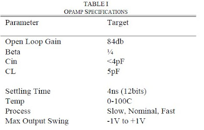
Abstract—This report presents a fully differential operational amplifier (opamp) for a pipeline analog-to-digital (ADC) with high gain (110 dB), ample phase margin (67.8°), low input capacitance ( 1.5 pf) and fast settling time (29.03ns) designed in a 2.5 V, 0.250 um CMOS process. The opamp consumes 59.2mW of power and 800um x 400um of area. The opamp’s performance was verified over 0-100 C and three process corners.

Index Terms—common mode feedback, gain enhancement, opamp, pipeline ADC

I.    INTRODUCTION

HIS report presents a fully differential opamp designed for a pipeline ADC stage. Table 1 highlights the specifications for the design. The implementation of this design must have high gain and a fast settling time. The quickness of opamp settling determines the speed of the pipeline ADC, thus fast settling is desirable. The higher the gain of an omamp the more ideal it is, and in feedback gain approaches 1/β with less error. [1] presents a design with high gain and high unity gain bandwidth though their implementation was in a significantly different process than ours. The authors present a differential folded cascode amplifier with gain enhancement, as well as presenting relevant background on gain enhancement. The authors were able to achieve a gain in excess of 90 dB, which exceed the specification for our project. We therefore chose the enhanced folded cascode architecture as the basis of our design

The folded cascode provides the needed headroom for an output swing in excesss of 1Vpk. With enhancement a high gain is possible, as [1] showed.

III.    CIRCUIT DESCRIPTION

A.    Architecture


Figure 1 highlights the architecture of the opamp that was  designed. A fully differential in and out amplifier was

realized. A folded cascode differential amplifier was chosen in order to support the specified output swing of 2 volts peak to peak.. The folded cascode design was also selected for its high output impedance. Bias current is mirrored with PMOS devices across the top of the schematic. Gain enhancement boost amps were designed and implemented to increase the output impedance of the folded cascode and meet specified gain. PMOS inputs were selected to minimize the capacitance at the drain node of the input devices, as NMOS are more area efficient, to improve phase margin. Bias voltages are generated in the block I33 using ratios of NMOS and PMOS sizing. Finally, common mode feedback was implemented in order to improve output swing. 
 
B.    Gain Enhancement


Figure 2 highlights the architecture of the gain enhancement that was implemented. A differential in single ended out opamp with gain A works to resist changes in the gate source voltage of M2 increasing the effective output resistance of the cascode of the by A. The gain enhancement also adds robustness to temperature and process variation. The gain boost opamp positive terminal takes a reference voltage that can be selected to ensure the drain source voltage of M1 remains large enough to ensure M1 stays in the saturation region which gives the highest output impedance.


The gain boost amplifiers were implemented with single ended output folded cascode opamps as shown in [4].

D.    Common Mode Feedback

Common mode feedback is necessary to regulate the common mode of the differential outputs of the opamp to ensure a large output swing. In figure 1 the common mode feedback circuit block is within the center of the two halves of the folded cascode. A simplified schematic of the common mode feedback circuit can be seen in figure 3. The current sources in the figure represent the pmos current mirrors. Vout+ and Vout- are the outputs of the enhanced folded cascode. Vset is a reference voltage that needs to be insensitive to temperature and process variations, to ensure constant common mode output. Vset is generated using two equally sized NMOS as a voltage divider to set VSET ideally to half of VDD. The diode connected NMOS is used to mirror current back into the folded cascode stack.

The circuit operates as follows: as the output common mode rises more of the current from the current sources is sunk through the outside legs of the circuit, and thus through the diode connected NMOS current mirror at the bottom of the circuit. This increase in current through the NMOS causes an increase in current within the folded cascode stack, forcing the output common mode to fall. Thus a form of negative feedback exists that regulates the output common mode.

IV.    CIRCUIT ANALYSIS

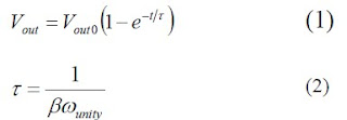
The most challenging target specification was the 12bit settling time of 4ns. According to equation (1) and (2) a unity gain frequency of 1.3GHz is necessary to meet this specification.


Using our output capacitance specification of 5pF in equation (3) the required gm of the input PMOS was calculated to be 6.5mS.


Using the gm of 6.5mS, we solved for the output impedance necessary in a non-boosted folded cascode to obtain a gain of 84dB. Drain current values through the drivers and the cascode devices were found using simplified hand calculation expressions for gm and rO and assuming all devices would operate in saturation. Device were initially sized using the MOSFET current equation and the drain current values that we calculated.

When this design was initially implemented, all devices operated in the correct region but gain, at approximately 40dB, was much lower than required. Common mode output voltage was also around 2V for each half circuit which would not allow the circuit to swing over the output range we desired. To overcome these shortcomings gain boost amplification and common mode feedback was added to the circuit. Design of the boost amps was based off of the sizings already generated for the fully differential circuit, but with current mirroring between half circuits to make the design differential in / single ended out. Design of the common mode feedback was based on of the NMOS folded cascode CMFB used in [2].

Implementation of CMFB and gain boosting gave us a circuit with an output DC voltage of around 1.25V which allowed the output to swing farther than required. It also resulted in a surplus of gain, producing around 120dB. Our unity gain frequency started out at around 250-300MHz in our intial design when driving the 5pF load cap. Increasing gm of the input transistor was used initially to raise this value, but when used alone the sizing of this device became impractical and capacitive loading of internal nodes by this device became pronounced. To push out ωunity we systematically scaled down the lengths and overall W/L ratios of devices connected to the output node and the intermediate cascode node. This allowed us to achieve a nominal ωunity of around 850MHz into the 5pF load with good single pole behavior throughout the amplifiers frequency response. An optimal input driver size was found such that scaling the driver down hurts performance and scaling the driver up yields no significant gains and a large area and power consumption cost.

To achieve stability and an acceptable phase margin the unity gain frequency of our boost amps needed to be slowed from their initial state. This was accomplished by attaching a capacitive load of 4.5pF to the output of each boost amp. This did not negatively affect overall ωunity and gave us a good 60-70 degree worst case stability (β = 1) phase margin for the overall circuit.

Our final design was very robust overs changes in bias voltage so biases were set with simple resistive divider circuits using diode connected PMOS and NMOS devices. The most important bias voltage for op-amp operation was Vset, the input voltage to the common mode feedback. This voltage was set using a divider of two identical diode connected NMOS devices so it does not depend on an N to P ratio to set its value.

V.    RESULTS

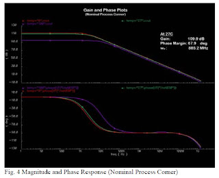
The fully differential opamp was designed in Cadence and simulated over slow, nominal, and fast process corners and at 0°, 27°, and 100° C. Layout of the device was also completed, and all presented results include extracted parasitics. Figure 4 below shows the open loop magnitude and phase plot. A fully differential frequency dependant input was swept to determine gain, unity gain freq, 3 dB bandwidth, and phase margin. Phase margin was measured for unity gain feedback to measure worst case stability. Simulated gain exceeded the target of 84 dB, with a value of 110 dB at 27 C. Unity gain bandwidth was 885 MHz which is less than 1.3 GHz target for a theoretical 12 bit settling time of 4 ns, for nominal process and 27 C.

Transient analysis was also completed to measure output swing, and settling time. Transient analysis was completed with inverting feedback with a feedback factor of ¼, as shown in figure 5. Ideal feedback was implemented by using a voltage controlled voltage source with unity gain to decouple the output of the opamp from the feedback network. A resistive divider network of 1kΩ and 3kΩ, giving a beta of ¼ and an ideal gain of 3. Figure 6 shows a transient response focusing on the rising edge of the output for a differential switch in the input. There is not ringing in the output as expected for a unity gain feedback phase margin of 67°. Phase margin > 60° was achieved for all process corners and temperatures. This the opamp has sufficient phase margin to ensure stability. The feedback factor of ¼ also adds to this stability. (Add schematic) Settling time was measured over all process corners and 0,27, and 100 °C. The 12 bit settling time for the average case (27 °C, nominal process) was measured with the settling time calculator in Cadence to be 29.03 ns. The best 12 bit settling time measured was 17.99 ns (0 °C, nominal process). The worst 12 bit settling time measured was 91.65 ns (0 °C, slow process). All measured settling times were greater than the target of 4 ns for this project.

The output swing specification of 1 Vpk was met over all process corners and temperatures. Output swing was verified by checking to ensure that the opamp was not railing out and that an output swing greater than 1 Vpk could be achieved. Figure 7 shows an output swing greater than 1 Vpk (27 °C, nominal process). Stability of the opamp at this operating point is also evident. Table II highlights the 10 bit settling time, unity gain bandwidth, gain, and phase margin over all temperature and process corners considered. Target settling time of 4 ns for 12 bits was specified, but 10 bit settling time was also measured with cursors in Cadence. Data is reported to show variance with process and temperature.
Table III provides a performance summary of the opamp for the average case (27 °C, nominal process).

Figure 8 shows the device layout. It closely follows the schematic and fits in an area of 800umx400um. Routing is restricted to metals 1 through 3 avoids routing over devices. The layout is DRC and LVC clean. 


VI.    CONCLUSION

A fully differential opamp for a pipeline ADC was realized with an enhanced folded cascode opamp with high gain (110 dB), ample phase margin (67.8°), low input capacitance ( 1.5 pf) and fast settling time (29.03ns) for nominal process corner, 27° C The opamp consumes 59.2mW of power and 800um x 400um of area.

The design met specs for output swing(>1 Vpk), input capacitance (<4pf), and phase margin(>60°) for all process corners and temperatures. Thus design was sufficient output swing and stability all tested operating conditions. The design exceeded the spec for gain (> 84 dB) for all process corners except for the case of slow process and 100°C. Thus gain is very stable over many operating conditions.

The design was unable to meet the target 12 bit settling time of 4 ns over any process corners and temperatures. This is where the design could be improved. This design would have better settling behavior or a smaller load cap. If there was room for greater input apacitance ore transconductance could have been realized increasing the unity gain requency and potentially further reducing the settling time.

Hernández Caballero Indiana
Asignatura: CAF
Fuente:http://www.eecs.umich.edu/~mpflynn/teaching/design_contest/fall_2005/reports/group4_eecs413_F05.pdf

COMMON MODE STABILITY IN FULLY DIFFERENTIAL VOLTAGE FEEDBACK CMOS AMPLIFIERS

ABSTRACT

In this study consideration is made of the common mode (CM) behavior of two-stage fully differential amplifiers in voltage feedback connection. In particular, interaction between internal CMFB circuitry and the external feedback network is investigated in order to highlight a possible operating point instability condition, due to the presence of a positive feedback loop. Two alternative CMFB topologies are compared, one of which is affected by instability, with development of constraints on the feedback network parameters to be fulfilled in order to avoid instability. Comparison was made by circuit simulations with reference to a low voltage, deep sub-micron CMOS technology (0.12 μm) implementation of a differential amplifier.

1. INTRODUCTION

Fully differential circuit structures are at present widely employed in low voltage (LV) applications, due to their improved immunity to noise, larger output swings and reduced distortion. However, these benefits are obtained at the expense of greater complexity, since differential amplifiers usually require internal common mode feedback (CMFB) loop in order to stabilize their d.c. voltages at both internal and output nodes. Although a great amount of work is currently underway which addresses this problem either by optimizing the CMFB loop in terms of linearity, speed, power consumption, and so on [1,2], or by trying to control the CM without employing any additional circuitry [3,4], no general solution is presently available since the variety of different situations arising in practical applications requires special approaches. This study shows that two distinct CMFB loops are generally active in a differential voltage amplifier with internal CMFB circuitry [5] and identify the conditions for which their interaction point at the amplifier power on. Fig.1 shows the schematic of a differential voltage amplifier implemented with a fully differential Opamp. One of the feedback loops, internal to the Opamp, includes the CMFB circuitry, while the other is made up of the external passive feedback network and the CM signal path of the Opamp. While the former achieves negative feedback, the latter is positive for a typical two-stage amplifier, and may cause instability.
 

In order to distinguish between the two loops, the former is referred to as ‘internal’, while the latter is ‘external’. According to this definition, Tint and Tex represent corresponding loop gains while V’icm, Vicm and Vocm are CM voltages at nodes 1-2, 3-4 and 5-6 respectively, as indicated in Fig.1.

2. ANALYZING THE CMFB LOOP


The problem can be studied in its essential aspects with reference to simple Miller Opamp architecture, although analysis can easily be extended to more complex situations including both telescopic and folded cascode topologies, circuits or opamps. An initial CMFB topology is analyzed here which sets up CM control by regulating gate voltage across M0, as shown in Fig.2. In this figure, ACMFB, which is negative, represents the voltage gain of the CMFB circuit, while M0 is in the saturation region. Apparently, the amplifier has a non-inverting common-mode gain, Acm, resulting as it does from cascade connection of two inverting stages. As a consequence, as has already been pointed out, a positive feedback effect arises when the external differential feedback network is connected which may affect overall amplifier stability. In fact, denoting the feedback factor by:
 

The external CM loop gain, Tex = Acm.f, must be kept smaller than unity so as to avoid instability.
 
 
In particular:

Where: Acm0 is the CM gain without the CMFB circuit and Tint is the internal CM loop gain. Defining the impedances at the drain of the cascode and output transistors by rp1 and rp2 respectively, Tint can be calculated from the CM half circuit of the amplifier shown in Fig.3:
 
 
As Acm0 has a low value due to the high CMRR of the Opamp, Acm will normally be very small.

However, with reference to the CM loop in Fig.2, an increase of the CM signal Vicm, at the input of the amplifier, may lead the transistor M0 to operate in its triode region, in which case the circuit assumes a nonlinear behavior since the M0 output resistance is no longer constant. Reducing output resistance of the tail current source will cause a decrease in CMRR and an increase in Acm0, with Tint also dropping owing to its proportionality to gm0. As a result, Acm increases along with Tex. The amplifier d.c. operating point is determined by the equilibrium condition resulting from the simultaneous action of both internal and external feedback loops. If V’icm = VREF = cost., the expression of the static characteristic of the external feedback network is simply:


Graphical representation of this relationship, with k= R2 / R1, is shown in Fig.4 (solid lines). The slope of these characteristics is 1/f. The dashed curve refers to the static input-output CM characteristic of the Opamp. The equilibrium condition must satisfy the constraints imposed by both characteristics and corresponds to the intersection of the two curves of Fig.4. Owing to the non-linearity of Acm, the equilibrium condition may not be univocally identified, also depending on the values assumed by the two resistors R1 and R2. In particular, a range [0, k*] exists, such that three distinct intersection points occur when 0 < k < k*, while a single equilibrium point exists for k > k*. For example, assuming VREF = 0.7 V and VDD = 1.5 V leads to a value of k* = 1.67 (obtained by setting Vocm = VDD and Vicm = VDD-VSG-VSDsat in eq. (2)). Thus even a simple, widely employed, voltage buffer (k = 1) may be affected by the described operating point ambiguity. Analysis of Fig.4 appears to indicate that for k within the interval [0, k*], points 1 and 3 correspond to stable equilibrium conditions, since they refer to low values of Acm, while point 2 is unstable, since it occurs in correspondence with a high Acm value. This is also apparent from evaluation of the slope of the dashed line at point 2. Under these conditions, in fact, Acm> 1/f or, equivalently, Tex > 1. In order to check for the validity of the above conclusions, circuit simulations were carried out with reference to a low voltage deep sub-micron CMOS technology (0.12 μm) implementation of a differential amplifier. Values for VDD and VREF are  respectively 1.5V and 0.7 V. A voltage buffer configuration has been chosen: R1 = R2 = R, with CMFB circuit assumed to have a unity gain. 
 
 
The operating point ambiguity is apparent from analysis of the figure 5, which shows the CM static input-output characteristics of the open loop Opamp.


A graphical estimation of k* from Fig.5, gives a value of 1.92, not too far from that obtained by manual analysis. Figure 6 shows the transient CM output voltage of the feedback amplifier corresponding to an input triangular signal V’icm. The output signal waveform can be derived from the static characteristic in Fig.5, since input signal frequency is small enough to be considered as a static stimulation. For V’icm approximately equal to 1.2 V, the d.c. amplifier output sets to: Vocm = VDD (point 3 in Fig.4). Once in this erroneus operating condition, the circuit is unable to exit even when V’icm settles to VREF. In fact, setting Vocm = VDD in equation (2), we obtain Vicm = 1.1V which falls outside the CM input dynamic range of the Opamp, corresponding (Fig.5) approximately to the interval [0, 0.9V]. Simulation (Fig.6) confirms that the circuit leaves the operating point 3 for V’icm = 0.3V, obtained by evaluating VREF in eq. (2) for Vicm = 0.9V and Vocm = VDD.
 

3. ALTERNATIVE CMFB TOPOLOGY

A dissimilar CMFB topology is obtained by controlling the gate voltage across transistors M5- M6, rather than the Vgs of M0. Fig.7 shows the CM half circuit of the Miller Opamp of Fig.2 which employs the above CMFB topology. Evaluation of the internal CM loop gain Tint for the circuit in Fig.7 leads to the following expression:
 
In contrast to the previous case, Tint is now independent from gm0, guaranteeing that Acm and, consequently Tex, are within a relatively low value even when high CM input voltage is applied which reduces gm0. The value of ACMFB can be chosen so as to obtain the desired value of Acm, even though it must also satisfy stability constraints referred to the internal CM loop. Reduction of Acm over a wider range of Vicm well above VREF results in the elimination of the instability condition since no multiple intersection points will be allowed in the plots of Fig.4. Circuit simulations were again carried out under the same conditions as in Figs. 5 and 6, but with the adoption of the second CMFB network, with results presented in Fig.8 and Fig.9. 
 
 
Fig.8 shows that a single equilibrium point now exists for Vicm = 0.7 V. This result is also confirmed by transient analysis (Fig.9) since, in this case, the circuit does not enter an erroneous operating condition when stimulated with a full amplitude triangular waveform. However, for high values of the input signal, the output CM voltage Vocm drifts from its correct value, due to variation of the CM gain Acm, as is clearly in evidence looking at the slope of the solid line in Fig.8.
 

5.    CONCLUSIONS

This study shows that two distinct feedback loops are generally operating in a differential voltage amplifier with internal CMFB circuitry. The conditions under which their interaction does not allow for univocal determination of the d.c. operating point of the circuit have been identified. In particular, we related the presence of instability to the drop of the internal CM gain Tint for certain values of the input CM signal, which, in turn, increases the value of Acm and Tex. When comparison of the two different topologies of CMFB networks was carried out, only one solution was shown to be affected by instability. The validity of this analysis was checked by simulation with reference to deep submicron CMOS technology implementation.

Hernández Caballero Indiana
Asignatura: CAF
Fuente:http://richpc1.ba.infn.it/~atauro/politecnico/publications/cr1141.pdf

A 403-MHz Fully Differential Class-E Amplifier in 0.35 μm CMOS for ISM Band Applications

Abstract

This paper presents the design and implementation of a low voltage, high efficiency class-E power amplifier (PA) for ISM band applications at 403 MHz. The PA circuit consists of an on-chip differential amplifier including the buffer stage on standard 0.35μm CMOS technology. The output matching circuit is implemented by off chip passive components including an external balun. The post-layout simulation results indicate that the amplifier is capable of delivering 20.9 dBm of output power to a 50Ω load with 1.5V power supply. The results also indicate that the PA has a gain of 11.8 dB at 403 MHz with power added efficiency (PAE) of 75%. The overall efficiencyincluding the buffer is 65.6%.

1.    Introduction

The demand for single chip transceivers has motivated the design of power amplifiers in CMOS technology. Especially for short-range wireless applications that require moderate output power, CMOS amplifiers are the suitable choice. Various power amplifiers (PA) in CMOS technology have already been reported [1-4]. The mass fabrication cost of CMOS integrated circuits is relatively low; therefore, designing the whole system on a single chip is very cost effective. Considering the portable devices, an efficient power amplifier can provide long battery time. Therefore, increased efficiency is a prime requirement for future generation wireless systems. The major limitation with CMOS technology for high power applications is its low breakdown voltage and especially the situation is worse with deep submicron CMOS devices. However, with advancements in technology and the availability of high voltage CMOS transistors, this problem can be addressed. Thus, for wireless applications, with moderate power, CMOS is an appropriate choice. In this paper, a differential power amplifier is designed and implemented using standard 0.35 μm CMOS technology process. The paper outline is as follows. Section 2 briefly describes the operation and design principles of class-E power amplifier. Section 3 discusses the design and implementation details of the amplifier circuit. Simulation results are provided in Section 4 while the work is concluded in Section 5.

2.    Class-E operation

Switching power amplifiers theoretically achieve efficiencies as high as 100%, but have drawback of poor linearity. Such amplifiers are suitable for systems with constant envelope modulation schemes [5-6]. The class-E PA is the most attractive candidate in terms of circuit simplicity and high-frequency performance. Typical configuration of a Class-E power amplifier is shown in Figure 1.
 
Transistor M1 operates as a switch and its current is passed through an inductor called radio frequency choke (RFC). The capacitance CS is in parallel with M1 and the parasitic capacitance of transistor is included inCS . LFIL and CFIL comprise a tuned circuit in series with a reactive component jX and the load impedance Ropt . The switch is turned on and off periodically at the input frequency. The LFIL -CFIL filter is tuned to the first harmonic of the input frequency and only passes a sinusoidal current to the load Ropt. The reactive component jX introduces the appropriate phase shift between the output voltage and the switch voltage to obtain desired waveforms [7]. The load network is designed such that the voltage across the switch is kept low when the switch turns off and voltage across the switch is zero when the switch turns on. The component values of single ended class-E power amplifier can be computed by following set of equations [8-10]: 
 
 
Where VDD, Pout, ω, and Q are PA supply voltage, PA output power, PA resonant frequency and inductor Q factor respectively.

3.    Design & Implementation

The major limitation of the CMOS technology is low breakdown voltage (VDS). In class-E amplifiers, the stress voltage at drain is 3.6 times VDD, therefore it is necessary to choose a device with higher VDS. For our design, we have chosen a high voltage NMOS transistor from standard 0.35μm CMOS design kit. This transistor has a maximum break down voltage of VDS=5.5V, and hence, with 1.5V VDD the maximum stress voltage on drain of the transistor is within safe limits, i.e., 5.4V.

3.1.    Single ended class-E design

A single ended Class-E amplifier is shown in Figure 2. The circuit was optimized for an output power of 150 mW with an operating frequency of 403 MHz at a supply voltage of 1.5V. Simulation results indicate that the transistor width of 1800 μm is required in order to meet the output power requirements. The other component values were computed by (1-5) and finally optimized by CAD simulations.
 
3.2.    Differential class-E design

Using differential topology gives some benefits over single ended configuration, such as common mode noise suppression. As a consequence, the even order harmonics are not significant. Differential design doubles the output power when compared with a single ended amplifier. For the same supply voltage and output power, the requirement on transistor size is also reduced in differential designs. This produces less parasitic capacitances and relaxes current consumption of the amplifier. Figure 3 shows the schematic of differential amplifier. The large inductors LRFC and LFIL are implemented off chip along with the external balun.
 
 
3.3.    Buffer design

The width of amplifier transistor is as large as 1800 μm that produces high parasitic capacitances. Consequently, the input gate capacitance Cgs of the transistor becomes too large to be driven by the preceding stage of the amplifier. A buffer amplifier, in such cases is required to drive the amplifier. The buffer is designed by a chain of inverters connected in series to drive the large capacitive load of 6.864 pF. Each inverter is larger by a factor of K (tapering factor) than the preceding inverter. For known input and output capacitive loads, the optimum value of Kopt and total number of inverter stages required in the buffer chain can be determined. The input gate capacitance CL of the amplifier transistor is 6.864 pF. Total input capacitance of first inverter stage is 4 fF and the output capacitance of first inverter stage (unloaded) is 1.8 fF. Optimum number of inverter buffer stages N is calculated and results in N=6.7. A seven stage buffer is required to drive a load capacitance of 6.864 pF. However, the simulation results indicate that only a five stage buffer is sufficient as it does not degrade the performance. Sizes of each stage’s PMOS and NOMS transistors are tabulated in Table 1.
 
 
3.4.    Layout issues

On-chip realization of inductors LRFC and LFIL is not feasible as it occupies a large chip area. Therefore, external high Q inductors were used. The bond wire inductance is also taken into account. In differential architecture, the symmetry of on-chip components and dimensions of the interconnects play a very vital role in the performance to cater process variation. Since the design is a differential, it has two identical single ended circuits. The PA has potentially large currents in different parts of circuit, so wide and stacked interconnect structures are used. Transistors in the circuit have large sizes such as widths of 1800 μm. It is not viable to place such a large transistor in one dimension, as poly material has high resistivity than metal and becomes too resistive over long dimensions. Multi-fingers were used and folded for carving large transistors. The poly materials of the fingers are connected in parallel to significantly reduce the resistance. All drains of multi-fingers are interconnected to behave as one single drain. In a similar way, all sources are interconnected to provide one single source. To avoid cross-talk and interference at radio frequencies, different blocks are encapsulated with guard-rings. This helps isolating the blocks to minimize interference and decouple substrate noise. Adequate on-chip decoupling capacitors were also used. The layout for the differential amplifier is shown in Figure 4. The overall chip area is 0.56 mm2 (700x800 μm) including the pads.
 
 
4.    Simulation results

The circuit simulations were performed in Cadence®. A test bench is designed to simulate the performance of PA. Pre and post-layout simulations were carried out. 
 
 
Figure 5 shows waveforms at different nodes of the class-E PA after post layout simulations with RC extraction. Results indicate that the amplifier has a gain of 11.8 dB at 403MHz. Figure 6 shows power added efficiency (PAE) and output power as a function of input frequency. At 403 MHz, PAE of the PA is 75% and the output power is 125 mW. The overall efficiency including the buffer stage is 65.6%.
 

Table 2 shows the comparison of results with already reported similar power amplifiers.
 
 
5.    Conclusion

The design and implementation of a low voltage high efficiency fully differential class-E amplifier is presented. Some key implementation issues have also been discussed. The post-layout simulation results are encouraging and indicate that the amplifier has potential to deliver 20.9 dBm of output power to a 50Ω load with 1.5V power supply. The results also indicate that the amplifier has a gain of 11.8 dB at 403 MHz with power added efficiency (PAE) of 75%. The overall efficiency including the buffer is 65.6%.

Hernández Caballero Indiana
Asignatura: CAF
Fuente:http://www.ewdtest.com/conf/proc08/ewdts08-68.pdf

sábado, 24 de julio de 2010

A NOVEL FULLY-DIFFERENTIAL CLASS AB FOLDEDCASCODE OTA FOR SWITCHED-CAPACITOR APPLICATIONS


ABSTRACT

This paper presents a new single-stage fully-differential class AB folded-cascode operational transconductance amplifier (OTA) for low-voltage and fast-settling switched-capacitor circuits in pure digital CMOS technology. The proposed OTA employs class AB operation in both the input-stage and output current source transistors resulting in large slew rate, enhanced unity-gain bandwidth and DC gain. The method to build the class AB operation in the output current source transistors is very simple which does not need any extra circuit and power consumption. HSPICE simulation results are presented to show the usefulness of the proposed OTA’s structure.

1.   INTRODUCTION

Design of high performance analog circuits is becoming increasingly challenging with the persistent trend toward reduced supply voltages. The main bottleneck in analog circuits is the operational amplifier. Operational amplifiers are widely employed to drive large capacitive loads in many switched-capacitor applications such as the integrators, gain stages, etc. For high speed applications, fast-settling OTAs are required, which demand both high unity-gain bandwidth and slew rate. In class A OTAs the slew rate is limited by the bias currents. For example in folded-cascode OTA assuming equal currents of Ib in both input and cascode transistors, the slew rate can be considered as SR = 2Ib/CL, where CL is the load capacitor. So, a trade-off exists between the static power dissipation and the slewing behavior of a class A OTA. However, in class AB OTAs the slew rate is not limited by the quiescent currents since when a large input signal is applied, large currents are generated provided that the circuit is designed properly. In this paper a single-stage class AB folded-cascode OTA which employs class AB operation in both the input-stage and output current source transistors is proposed which results in large slew rate. This technique also enhances the OTA’s unity gain bandwidth and DC gain. Section (2) presents the proposed OTA structure. In section (3) circuit simulation results are discussed. Finally, conclusions are presented in section (4).

2.   PROPOSED OTA TOPOLOGY

Figure 1 shows the proposed OTA structure. It employs the class AB operation in both input-stage and output current source transistors. To build the input-stage class AB operation, the proposed OTA uses two matched input transistors M1 and M2 cross-coupled by two constant voltage sources generated by two flipped voltage follower (FVF) cells acting as DC level shifters [1, 2, 6]. FVF cells composed of Mc1-Mc6 are used to build the floating voltage sources due to their very low output resistance instead of the conventional common drain structures [3]. Under quiescent conditions, i.e. when no input signal is applied, the gate voltage of input transistors M1 and M2 is the same. In this case, VSG1 = VSG2 = Vb, and both transistors carry equal currents which are controlled by Vb. Vb can be chosen slightly greater than the MOS threshold voltage which results in low quiescent currents. When an input signal is applied, a large current is generated in one of the input transistors. If for instance vin+ increases and vin- decreases, the source voltage of M2 increases whereas the voltage at the source of M1 decreases by the same amount. So, the drain current of M1 decreases while the drain current of M2 increases. Hence, the maximum current of M1 and M2 is independent of quiescent current when an input signal is applied. To build the class AB operation in the output current source transistors, the gates of M9 and M10 are connected to those of Mc6 and Mc5, respectively, which results in large currents to flow during the slewing in one of cascade branches. If for instance, vin+ is greater than vin-, the drain current of M1 will be decreased while the drain current of M2 will be increased by the same amount. The drain current of Mc5 will be increased, and so M10, while the drain current of Mc6 and M9 will be decreased. On the other hand, it can be also explained that the gate voltage of M3 and M4, cmfb, will be increased due to the sudden increment of the drain current and voltage of M2 through coupling of the gate-drain capacitor of M4 as it is seen in Fig. 2(a). The drain voltage of M2 increases greatly due to the enhancement of its drain current which results in raising the gate voltage of M3 and M4 through the gatedrain capacitance of M4. So, the drain current of M3 and M4 will be increased as shown in Fig. 2(b). Hence, the current of M10 will be forced to the positive output node, vout+, and the negative output node will be discharged by the current of M3. It is worth to mention that the increased drain current of M4 will be provided by M2 since due to the sudden increment of drain voltage of M2, the transistor M6 will be forced to cut-off. A similar improvement in the value of slew rate is obtained when a large negative input signal is applied to the proposed OTA. Therefore, a large slew rate will be obtained during both the positive and negative OTA’s slewings.


If the gates of M9 and M10 are connected to a fixed bias voltage, their currents will be remained fixed during the OTA’s slewing. In this case, when a large positive input signal is applied to the OTA, the positive output node will be charged only by the DC bias current of M10. So, the slew-rate of the proposed OTA will be much larger than that of folded-cascode OTA which employs class AB operation only in its input transistors. The class AB operation of output current source transistors, M9 and M10, also enhances the OTA’s small signal DC gain and unity-gain bandwidth. When a small signal is applied to the OTA’s input, this signal also appears across the gate-source of output current source transistors, M9 and M10 through the FVF buffer cells, which in turn results in enhancing the DC gain of OTA. Also the effective transconductance of the input transistors are increased from gm1,2 to about gm1,2 + gm9,10 which enhances the OTA’s unity-gain bandwidth by the same amount. It is worth mentioning that the class AB operation of the input-stage results in doubling the effective transconductance of input transistors, and hence doubling the unity-gain bandwidth and DC gain.


The proposed OTA has the lowest power supply voltage requirement which is about VGS + Veff where Veff is the drain-source saturation voltage of an MOS transistor. To get a large output signal swing, a two-stage OTA can be utilized where the first stage can be the proposed OTA in this paper and the second stage is a common-source topology with a class AB operation. Cascode compensation and/or hybrid cascode compensation can be used to stabilize this two-stage OTA in fast-settling applications [4]. A simple switched-capacitor common mode feedback (CMFB) circuit such as proposed in [5] is used to define the common-mode voltage of output nodes of the proposed OTA.

3.   SIMULATION RESULTS

To verify the usefulness of the proposed OTA, it was designed using a 0.25μm BSIM3v3 level 49 mixed-signal CMOS models with HSPICE for a switched-capacitor integrator with sampling and integrating capacitors of 2.5- pF and 10-pF, respectively. The load capacitance was 10- pF and 7.5-pF in AC open loop and transient closed loop simulations, respectively. The designed device sizes and circuit parameters are shown in Table 1. Figure 3 shows the frequency response of the proposed OTA including the conventional folded-cascode OTA called OTA1 here and the folded-cascode OTA with class AB operation only in its input-stage called OTA2 here. The settling performance of all three simulated OTAs is shown in Fig. 4. A summary of the simulation results is shown in Table 2. In these simulations, equal values for the transistors’ dimensions and bias currents have been used. Simulation results show that the proposed OTA achieves unity-gain bandwidth of about three times that of the conventional folded-cascode (OTA1) and about two times that of the folded-cascode OTA employing class AB operation only in its input-stage (OTA2). Its settling time is much less than the other two topologies due to its large slew rate and also unity-gain bandwidth. The proposed OTA also achieves about 3.6-dB and 10-dB DC gain greater than the class AB input-stage and conventional folded-cascode OTAs, respectively. The slew rate of class AB input-stage OTA is about the same as that of the conventional folded-cascode since when a positive input signal is applied, its positive output node is charged only by the bias current of M10.


4.   CONCLUSION

In this paper a novel fully-differential class AB foldedcascode OTA was proposed. The proposed OTA topology offers enhanced slew rate, unity-gain bandwidth, and DC gain by employing a simple technique to build the class AB operation in the output current source transistors in addition to using the conventional class AB input-stage. The method to build the class AB operation in the output current source transistors is simply realized by proper connection between the input-stage and the output stage nodes with no extra transistors and power dissipation.


Hernández Caballero Indiana
Asignatura: CAF
Fuente:http://eng.ut.ac.ir/iclab/members/yavari/Papers/ICEE%2705_Yavari.pdf